
.png)

.png)








Search
 2026.07.23
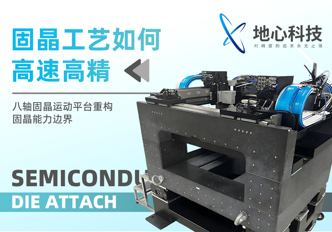
The Core of Advanced Packaging Production Line Upgrades: How Precision Motion Stages Enable High-Speed, High-Precision Die Attach Processes
.webp) 2026.06.03
2026.06.03
A Comprehensive Overview of the HBM Manufacturing Process: What Role Does the High-Precision Motion Platform Play?
A Comprehensive Overview of the HBM Manufacturing Process: What Role Does the High-Precision Motion Platform Play?A Comprehensive Overview of the HBM Manufacturing Process: What Role Does the High-Precision Motion Platform Play?
 2026.03.30
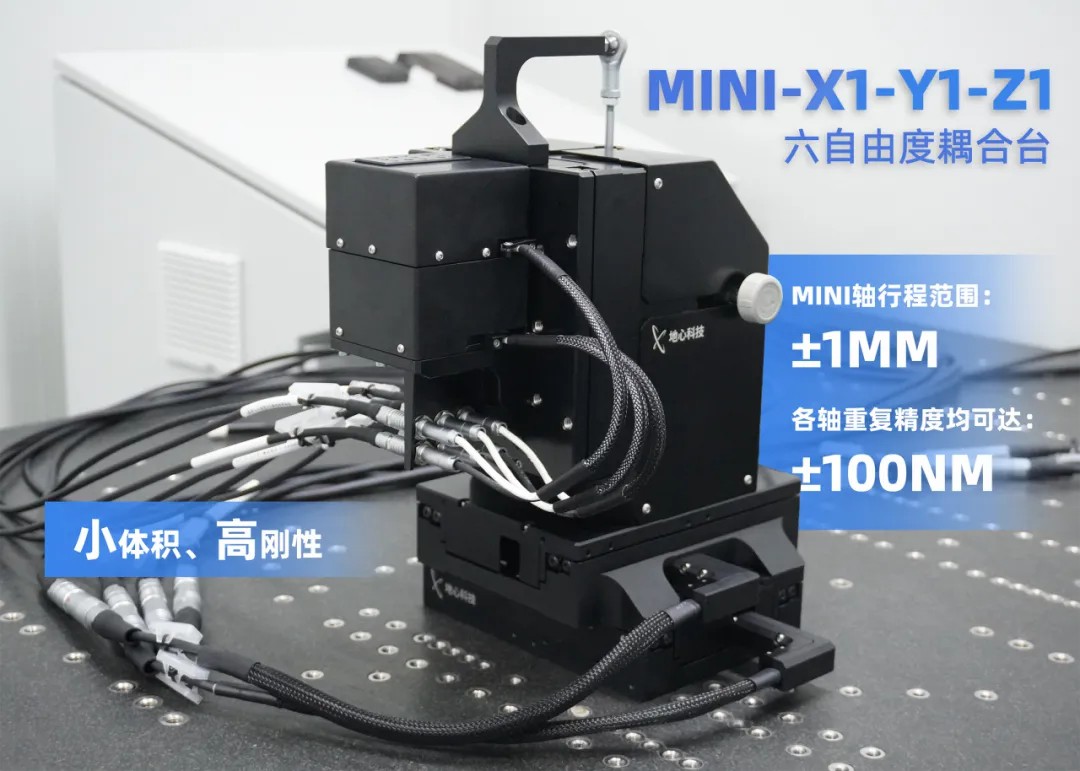
New Product Launch | At the Advent of 1.6T, Why Does the 6-DOF Optical Coupling Motion Stage Become the Key to Improving Efficiency and Reducing Cost in Optical Modules?
 2026.04.20
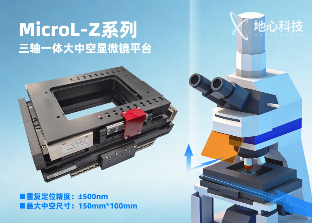
From "Seeing" to "Scanning with Precision": How Precision Motion Stages Drive the Industrial Leap of High-Throughput Microscopy Imaging
From "seeing" to "scanning with precision," high‑throughput microscopes are redefining the boundaries of life sciences and drug discovery at unprecedented throughput. Yet large‑area, nanometer‑level high‑precision imaging is inseparable from precision motion stages. From fast raster scanning to rapid Z‑axis focusing, the precision XYZ 3‑axis motion stage is the motion center that determines the imaging limits, operational efficiency, and long‑term stability of high‑throughput microscopy.
 2026.06.02
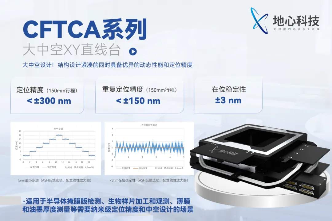
Semiconductor Photomask Inspection: Beyond the Optical System, High-Precision Motion Stages Also Determine True Accuracy
The error of a single photomask can be replicated onto thousands of chips.
To clearly see, accurately measure, and determine whether a photomask is qualified, relying solely on a high-performance optical system is far from sufficient. In a sense, the upper limit of photomask inspection is determined not only by optical precision, but also jointly by the precision, stability, dynamic response, and cleanroom compatibility of the motion stage.
To clearly see, accurately measure, and determine whether a photomask is qualified, relying solely on a high-performance optical system is far from sufficient. In a sense, the upper limit of photomask inspection is determined not only by optical precision, but also jointly by the precision, stability, dynamic response, and cleanroom compatibility of the motion stage.
 2026.04.28
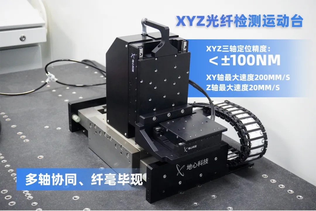
The Super Cycle of the Optical Fiber Industry Has Begun: Why Does Fiber Inspection Rely Even More Heavily on High-Precision Motion Stages?
![[Exhibition News] Riding the Wave of Precision Motion Control Once Again – Ground Motion Technology Makes a Stunning Appearance at Laser World of Photonics China!](https://www.coretech-revolution.com/en/uploads/images/202605/sgfaasfgf.jpg) 2026.03.23
2026.03.23
[Exhibition News] Riding the Wave of Precision Motion Control Once Again – Ground Motion Technology Makes a Stunning Appearance at Laser World of Photonics China!
From March 18–20, Laser World of Photonics China was grandly held at the Shanghai New International Expo Centre. Ground Motion Technology made a brilliant appearance with its latest motion stage developments and market‑proven motion control solutions. The booth attracted high foot traffic throughout the show, drawing numerous industry experts, long‑standing clients, and new customers for engaging discussions in a vibrant atmosphere.
![[Exhibition Invitation] Groundbreaking New Product Makes Its Offline Debut – Ground Motion Technology Invites You to Join Us at Laser World of Photonics China!](https://www.coretech-revolution.com/en/uploads/images/202605/gsdgsdsfd.png) 2026.03.05
2026.03.05
[Exhibition Invitation] Groundbreaking New Product Makes Its Offline Debut – Ground Motion Technology Invites You to Join Us at Laser World of Photonics China!
 2025.12.31
Chasing Light and Electrons, Iterating and Advancing | Inviting You to Join Us in Unveiling Ground Motion Technology's 2025 Milestones
.webp) 2026.06.02
2026.06.02
Beyond Cost and Energy Advantages: How Precision Motion Stages Further Enhance Nanoimprint Lithography Accuracy
Compared with EUV lithography, Nanoimprint Lithography (NIL) takes a different path. By leveraging the core principle of physical embossing combined with material curing, it significantly reduces process cost and energy consumption. However, NIL technology still faces considerable challenges in defect control during the manufacturing process, which limits its broader adoption. Precision motion stages may well be the key factor in breaking this deadlock.
.webp) 2026.06.02
2026.06.02
Behind the Mass Production of Hybrid Bonding: How Precision Motion Stages Meet the High-Precision Control Demands of Semiconductor Packaging
As the semiconductor industry advances toward smaller process nodes, traditional packaging technologies can no longer meet the demands of high-performance chips in terms of integration density, signal transmission, and energy efficiency. Advanced packaging technologies such as Heterogeneous Integration (HI), Chiplet, and System-in-Package (SiP) are increasingly becoming industry focal points, and these technologies impose stringent requirements on packaging accuracy.
.webp) 2026.06.03
2026.06.03
One Article Summary | Multiple Applications of Precision Motion Stages in Wafer Defect Inspection
 2026.06.03
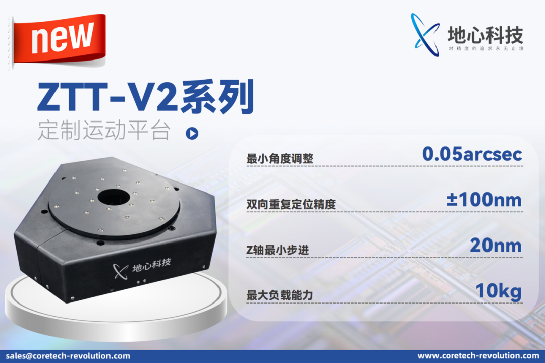
ZTT‑V2 Three‑Axis Tip‑Tilt Stage: Real‑Time Height and Angle Adjustment to Boost Precision Across Multiple Industries
.webp) 2026.06.03
2026.06.03
Improving Yield and Efficiency: High‑Precision Motion Stages Empowering Innovation in Laser Direct Writing Technology
.webp) 2026.06.03
2026.06.03
From Optical Chip Manufacturing to Fiber Coupling: Ultra‑Precision Motion Control Platforms Enabling a Technological Leap in the Optical Communications Industry
.webp) 2026.06.03
2026.06.03
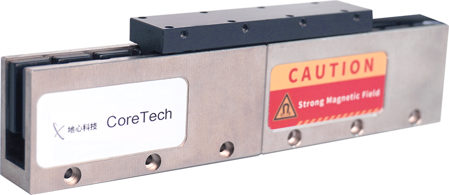
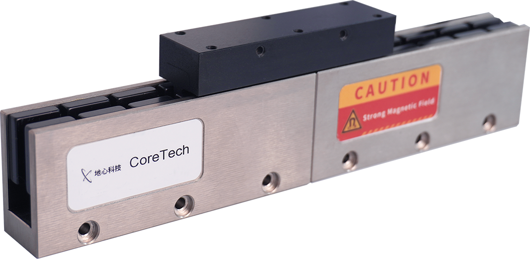
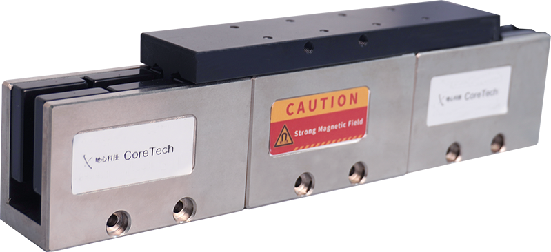
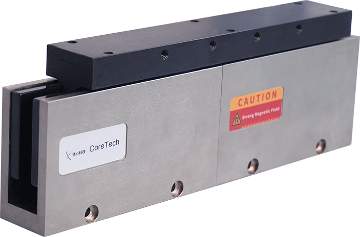
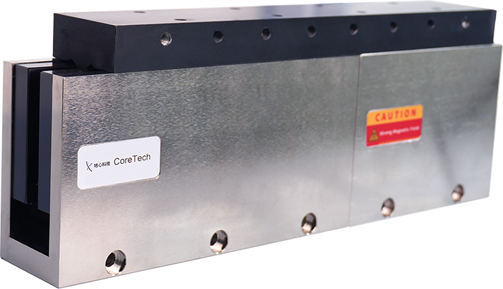
CORETECH's New-Generation Linear Motors: Ultimate Performance Reshaping Industrial Precision
.png) 2026.06.03
2026.06.03
Breaking the Boundaries of Chip Yield Improvement: Geocentric Technology's Wafer Spiral Inspection Solution Accelerates Quality and Efficiency in the Industry
.webp) 2026.06.03
2026.06.03
Medical Laser Processing of Heart Stents and Catheters: An Efficient, High-Precision Solution
.webp) 2026.06.03
2026.06.03
ASP Series Ultra‑High‑Speed, High‑Precision Air‑Bearing Rotary Stage – Maximum Speed 5000 RPM
.webp) 2026.06.03
2026.06.03
Coretech Application | Large Aperture 2D Motion Stage Enhances Reticle Inspection Accuracy in Mask Lithography
.webp) 2026.06.03
2026.06.03
3D Scanning Imaging of Brain Neural Networks: High-Precision Motion Stages Enhancing Accuracy and Efficiency
.webp) 2026.06.03
2026.06.03
High-Precision Motion Stages Enhancing Coupling Alignment Accuracy in Precision Fiber Coupling Equipment
.webp) 2026.06.03
2026.06.03
In Micro/Nano Direct-Write Lithography Systems, the Stage's Exceptional Dynamic Performance Enhances Lithography Accuracy and Efficiency
.webp) 2026.06.03
2026.06.03
Gene Sequencing: Solving Auto‑Focus and Equal‑Interval Triggering Issues to Enhance Measurement Accuracy and Efficiency
.webp) 2026.06.03
2026.06.03
Wafer Defect Inspection: Solving the "Auto‑Focus Tracking" Challenge to Improve Detection Accuracy and Efficiency
.webp) 2026.06.03
2026.06.03
Wafer Defect Inspection: Solving the "Spiral Motion Trajectory" and "Equal Arc-Length Triggering" Challenges
.webp) 2026.06.03
2026.06.03
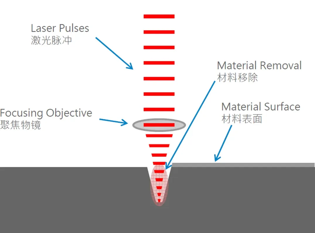
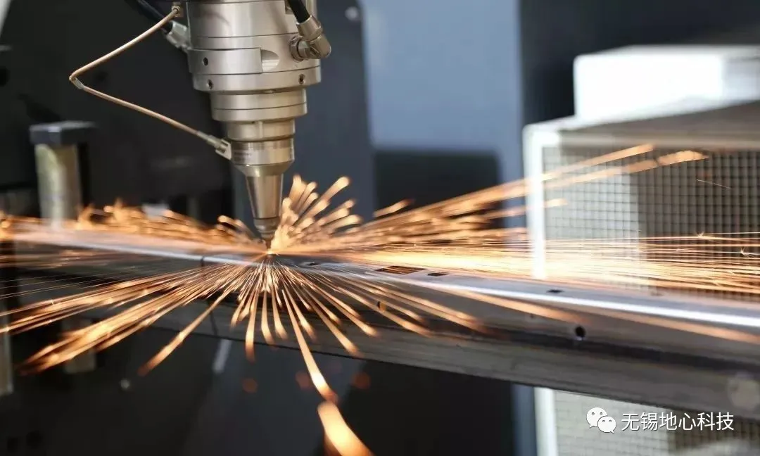
Laser Processing Automation Solutions – Laser Direct Writing and Plate‑Making Lithography
.webp) 2026.06.03
2026.06.03
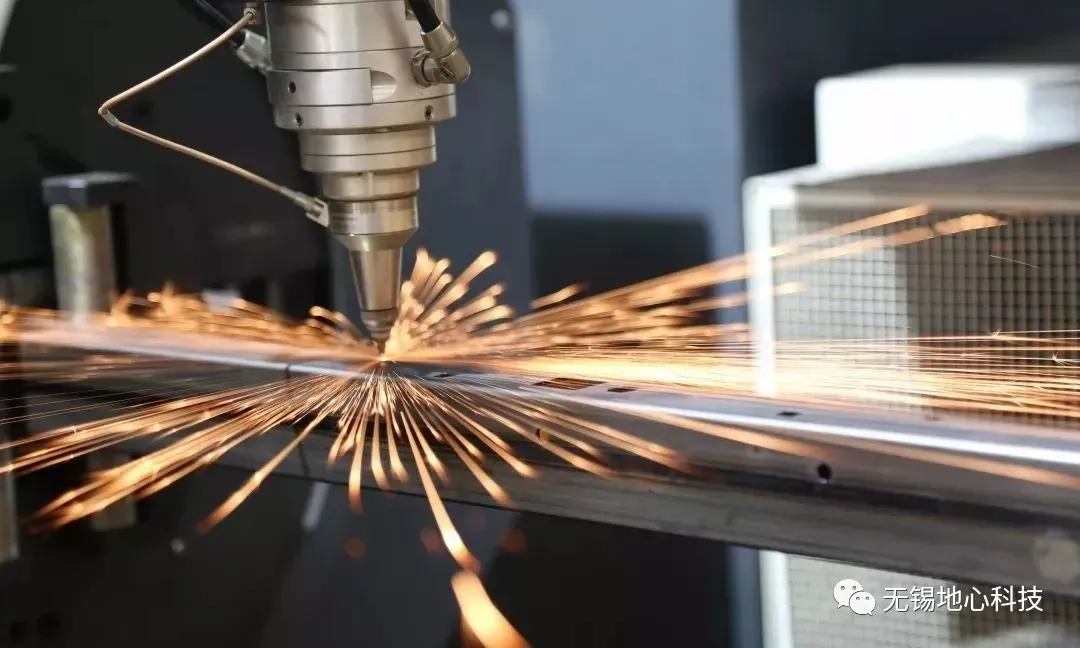
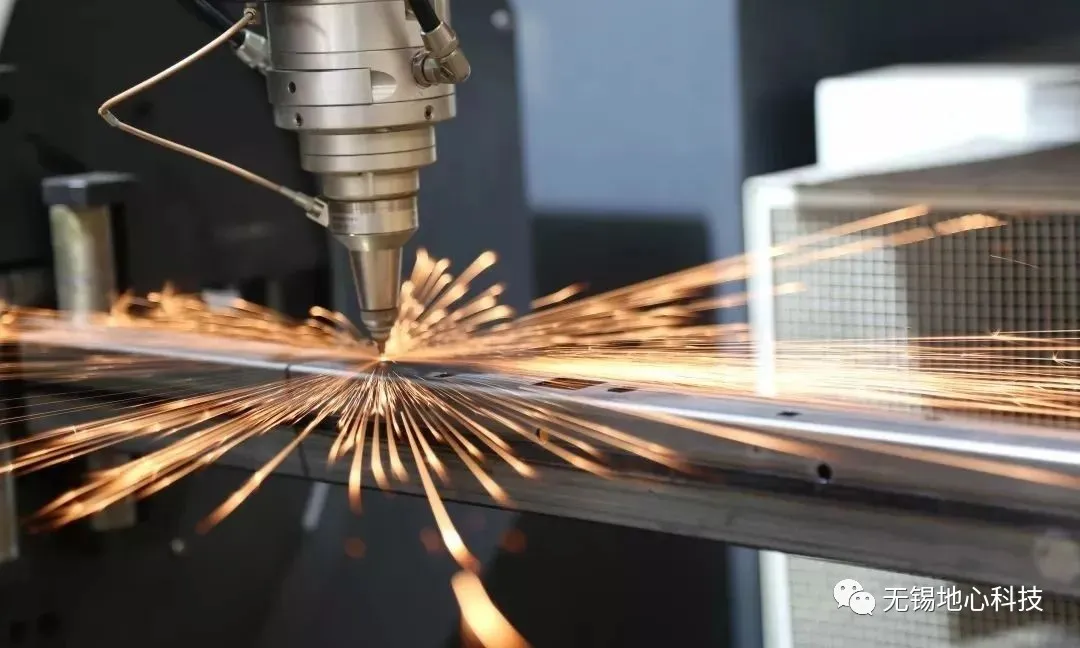
Semiconductor Wafer Inspection & IC Packaging Solutions – Die Bonder / Pick‑and‑Place Machine
.webp)
 2026.06.03
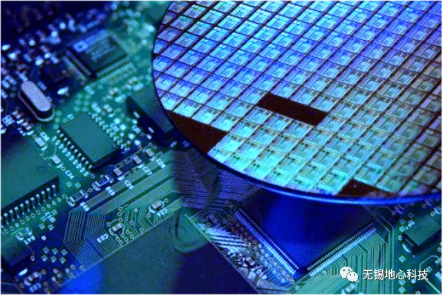
Semiconductor Wafer Inspection & IC Packaging Solutions – Photonic Chip and Optical Waveguide Processing
.webp) 2026.06.03
2026.06.03
Semiconductor Wafer Inspection & IC Packaging Solutions – Sensor Chip Testing