
.png)

.png)







Home
 News Center
Breaking the Boundaries of Chip Yield Improvement: Geocentric Technology's Wafer Spiral Inspection Solution Accelerates Quality and Efficiency in the Industry
News Center
Breaking the Boundaries of Chip Yield Improvement: Geocentric Technology's Wafer Spiral Inspection Solution Accelerates Quality and Efficiency in the Industry
News Center
Breaking the Boundaries of Chip Yield Improvement: Geocentric Technology's Wafer Spiral Inspection Solution Accelerates Quality and Efficiency in the Industry
Breaking the Boundaries of Chip Yield Improvement: Geocentric Technology's Wafer Spiral Inspection Solution Accelerates Quality and Efficiency in the Industry
 2026-06-03
Share:


01 Market Background
With the acceleration of global digital transformation and the explosive growth in fields such as 5G communications, artificial intelligence, and high-performance computing, increasingly stringent requirements are being placed on the performance, integration density, and reliability of integrated circuits.
As a critical link in ensuring chip yield and performance, semiconductor wafer inspection is deeply intertwined with industrial development through its technological innovations. Against this backdrop, the market demand for semiconductor inspection equipment continues to rise, with technological evolution and market needs showing a strong positive correlation.

Figure 1: Wide-ranging applications of semiconductors in daily life
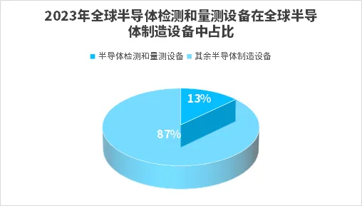
Figure 2: Global semiconductor inspection and metrology equipment as a percentage of global semiconductor manufacturing equipment in 2023
02 Customer Pain Points
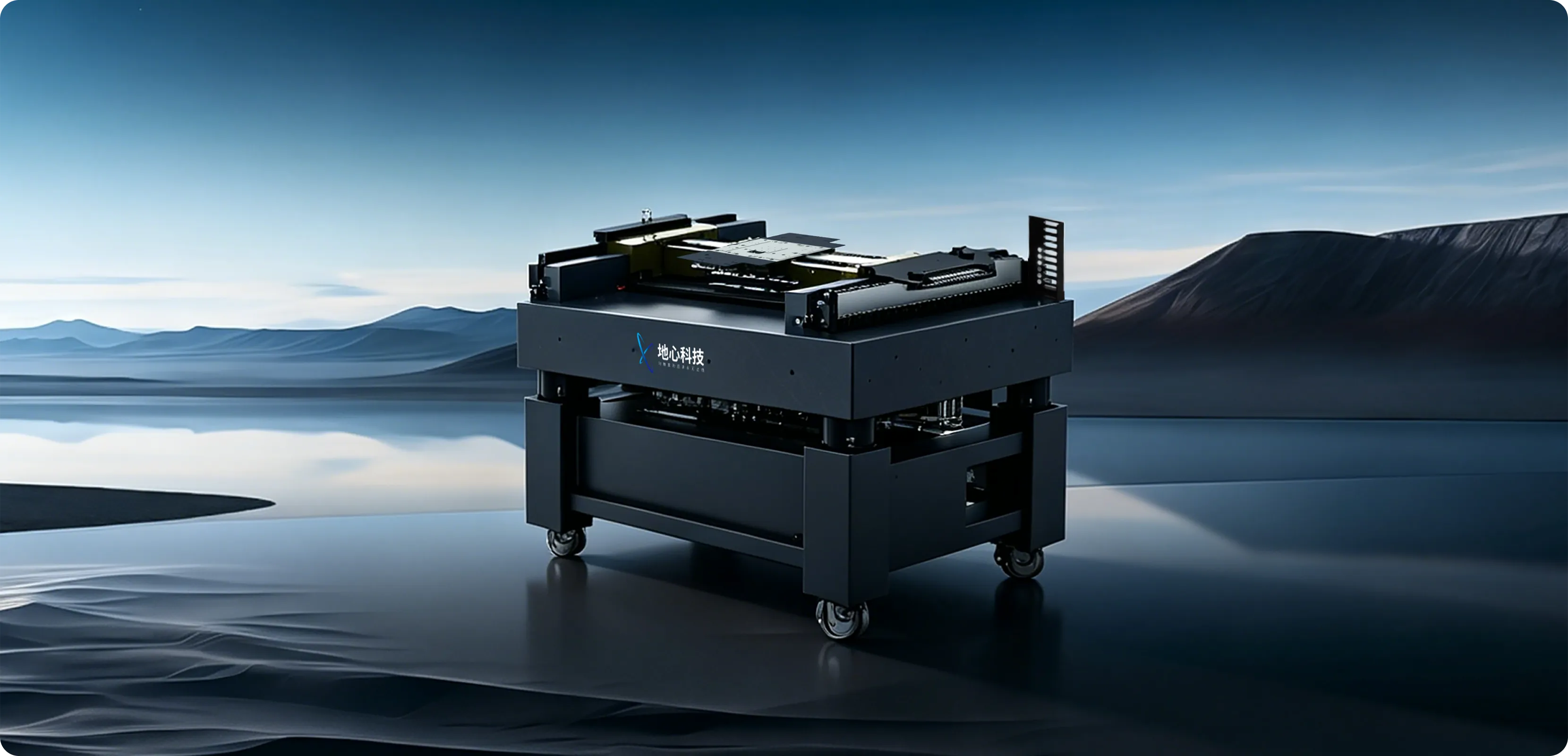
Technological breakthroughs in semiconductor wafer inspection directly determine the upper limits of chip yield improvement. Taking 7 nm and more advanced process nodes as an example, the number of inspection points required per wafer has increased by a factor of 4.1 compared with the 28 nm node, imposing much more demanding requirements on the accuracy and efficiency of motion control platforms.
Conventional inspection equipment generally adopts a raster‑type motion path (i.e., alternating reciprocating motion of the X and Y axes), which suffers from three major bottlenecks:
Low efficiency: Raster paths require multiple traversals to cover the wafer surface, with idle travel accounting for approximately 40% of the total movement. The inspection cycle struggles to keep pace with production line takt times.
Limited accuracy: Frequent start/stop and direction changes not only induce mechanical vibrations that affect optical system stability, but also require substantial settling time to bring the positioning error within acceptable limits.
Insufficient adaptability: The complex morphology at wafer edges (e.g., etched patterns, dicing marks) tends to create inspection blind spots. Conventional paths cannot dynamically adjust scan density, leading to higher escape rates.
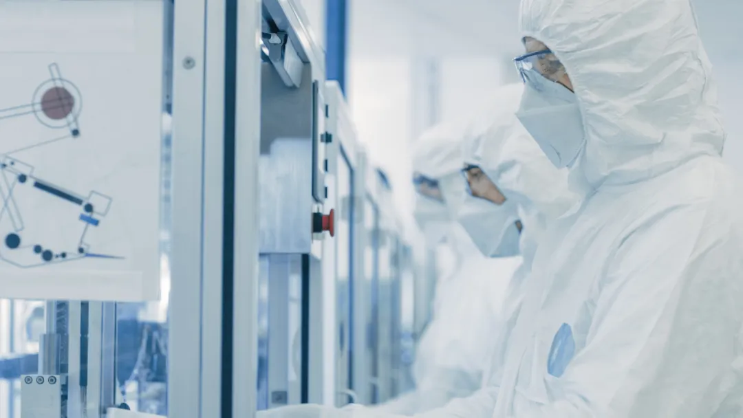
As a leading provider of industrial vision-based intelligent inspection equipment and solutions, a well‑known industry frontrunner had developed a series of wafer defect inspection systems and established collaborations with multiple key customers in the semiconductor sector. However, when serving customers with sub‑7 nm process nodes, they encountered critical challenges:
Low inspection efficiency
Defocusing caused by surface variations resulting from force changes, rotary‑stage axial/radial runout, or linear‑stage flatness deviations
Image blurring induced by disturbances from the high‑speed rotary stage to the linear axes
03 Solution
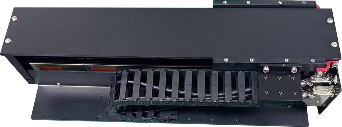
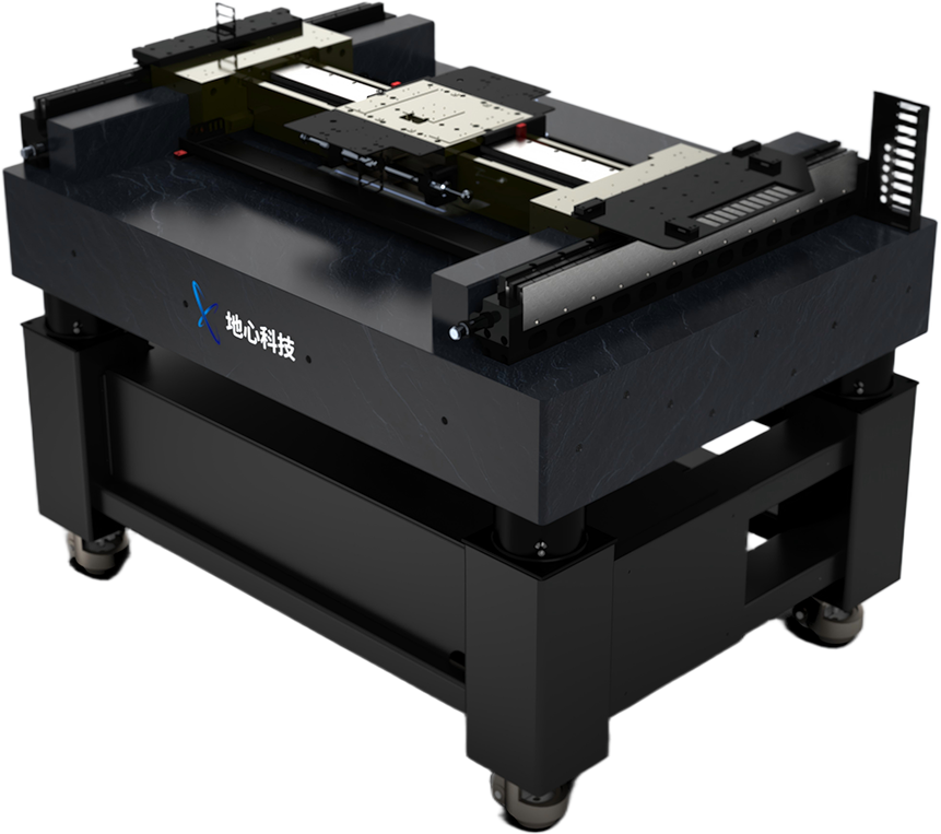
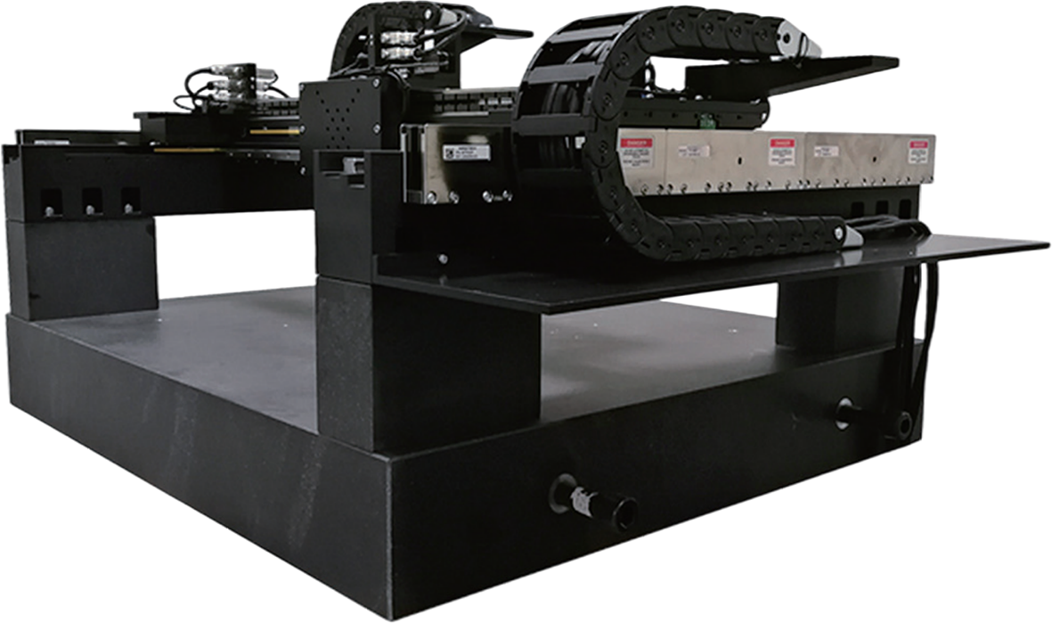
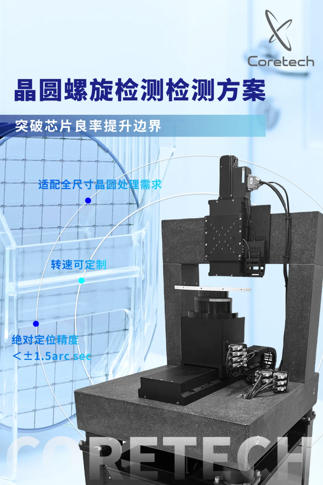
The spiral motion's inherent continuous‑path characteristics enable full‑wafer coverage in a single scan, reducing mechanical movement time by approximately 40% compared with conventional raster motion. Geocentric Technology's spiral inspection solution incorporates several key technological breakthroughs:
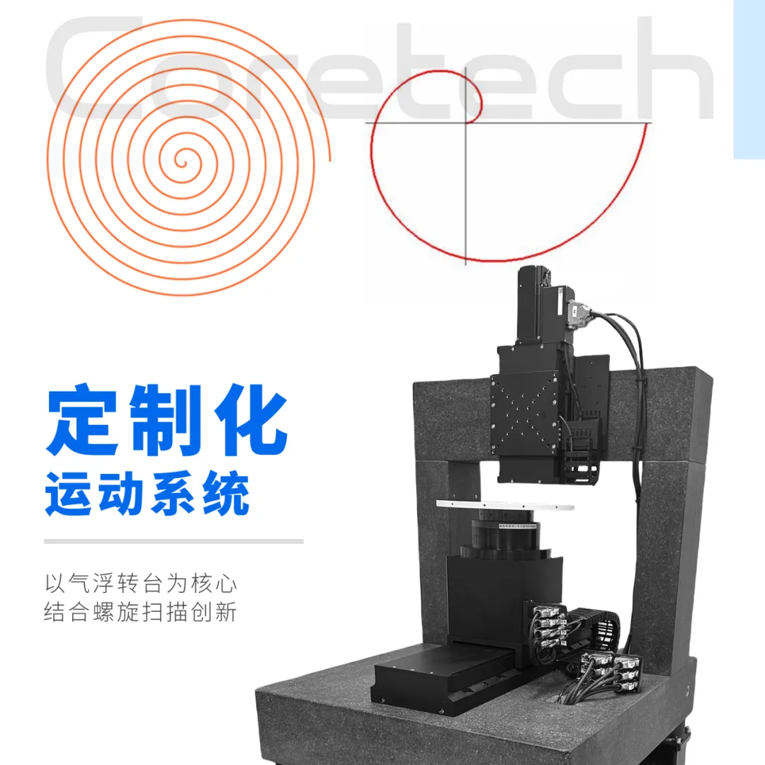
Figure 3: Typical spiral motion trajectory
Precision Distance Control
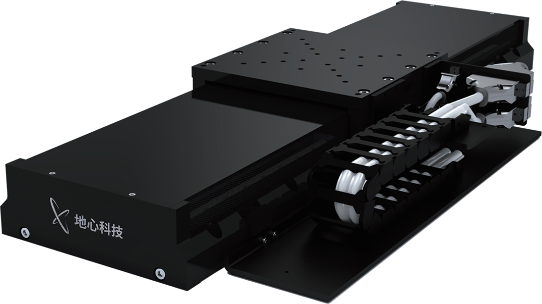
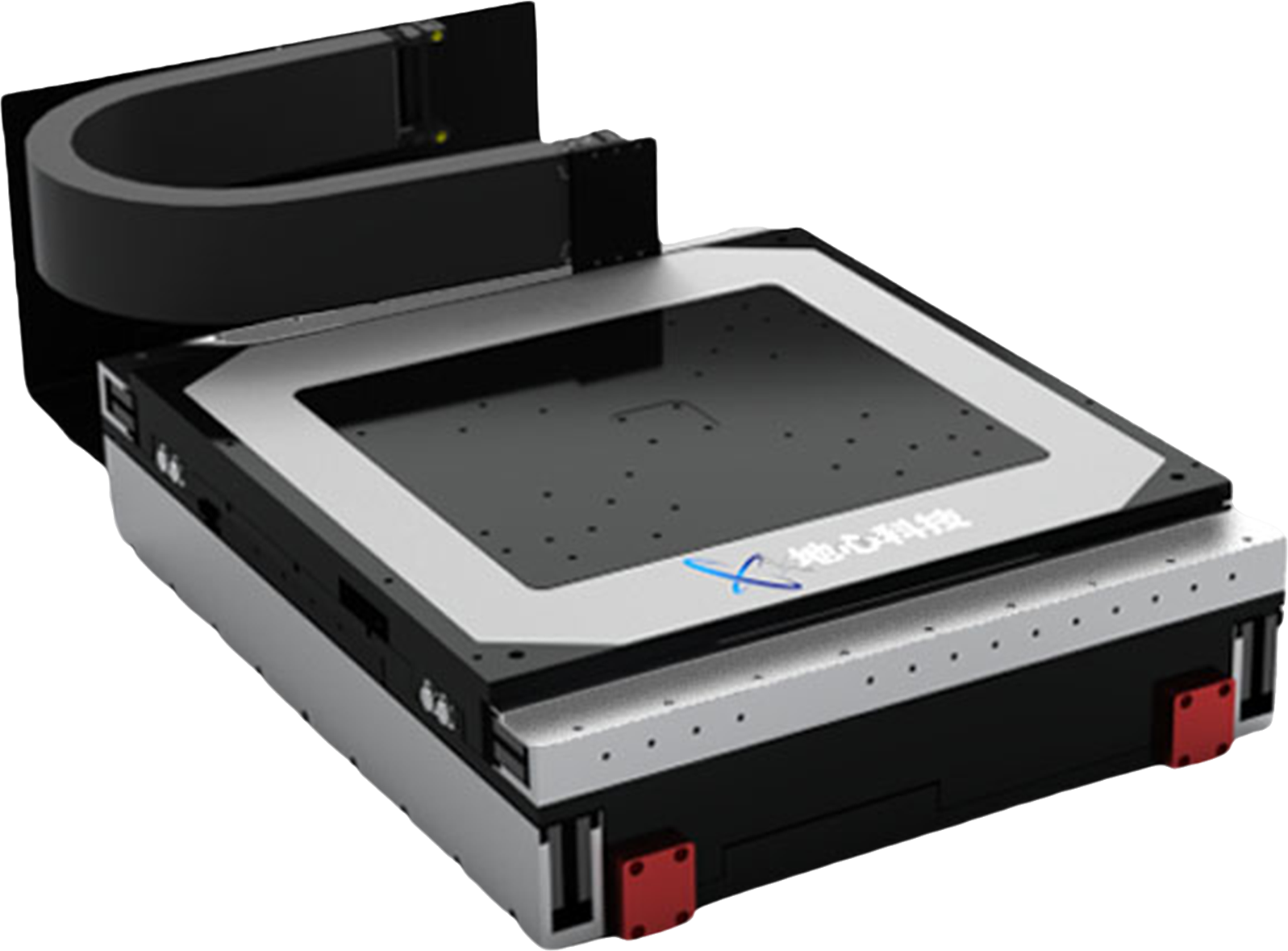
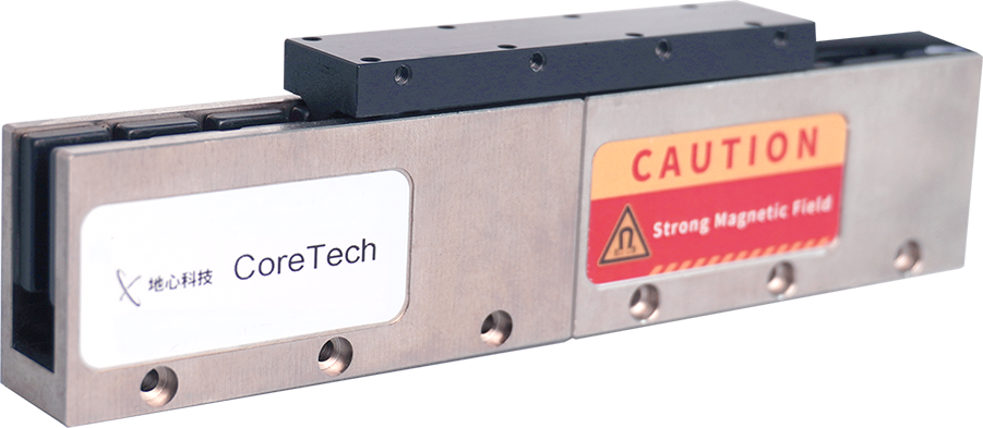
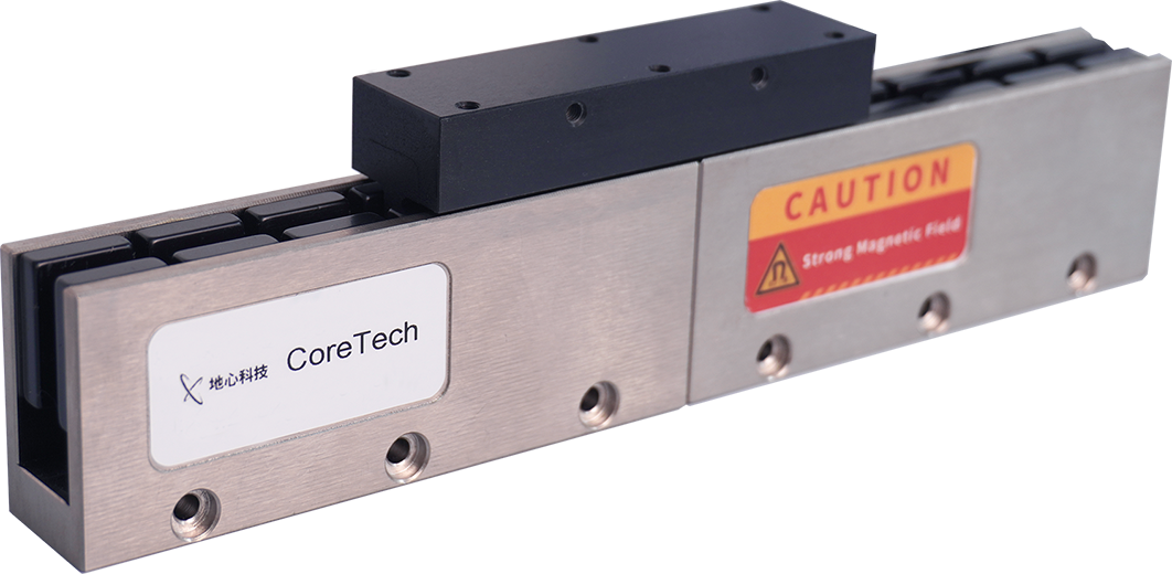
A Z‑axis stage with nanometre‑level positioning accuracy (self‑developed linear motor + cross‑roller guides) ensures a constant distance between the sensor and the wafer surface through high dynamic accuracy, achieving a no‑load cutoff frequency exceeding 200 Hz.
Motion Stability Assurance
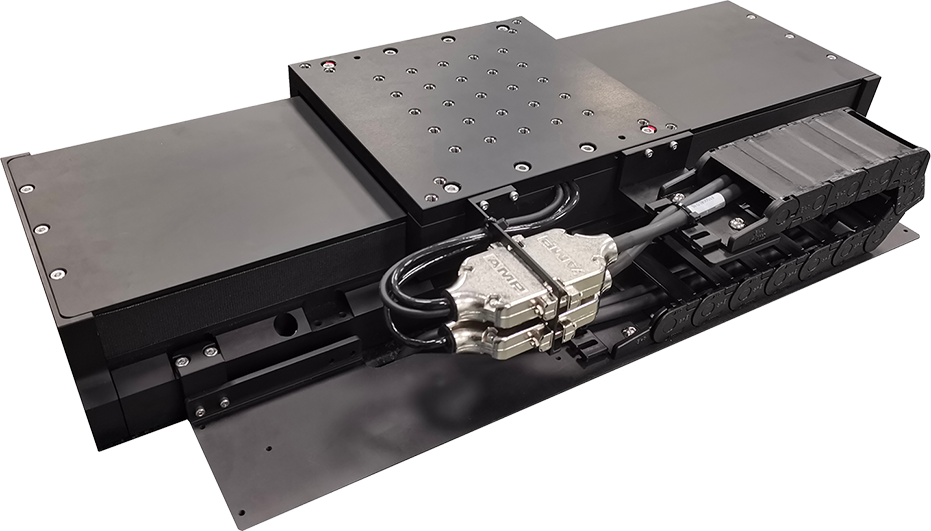
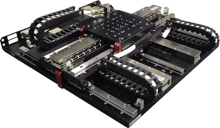
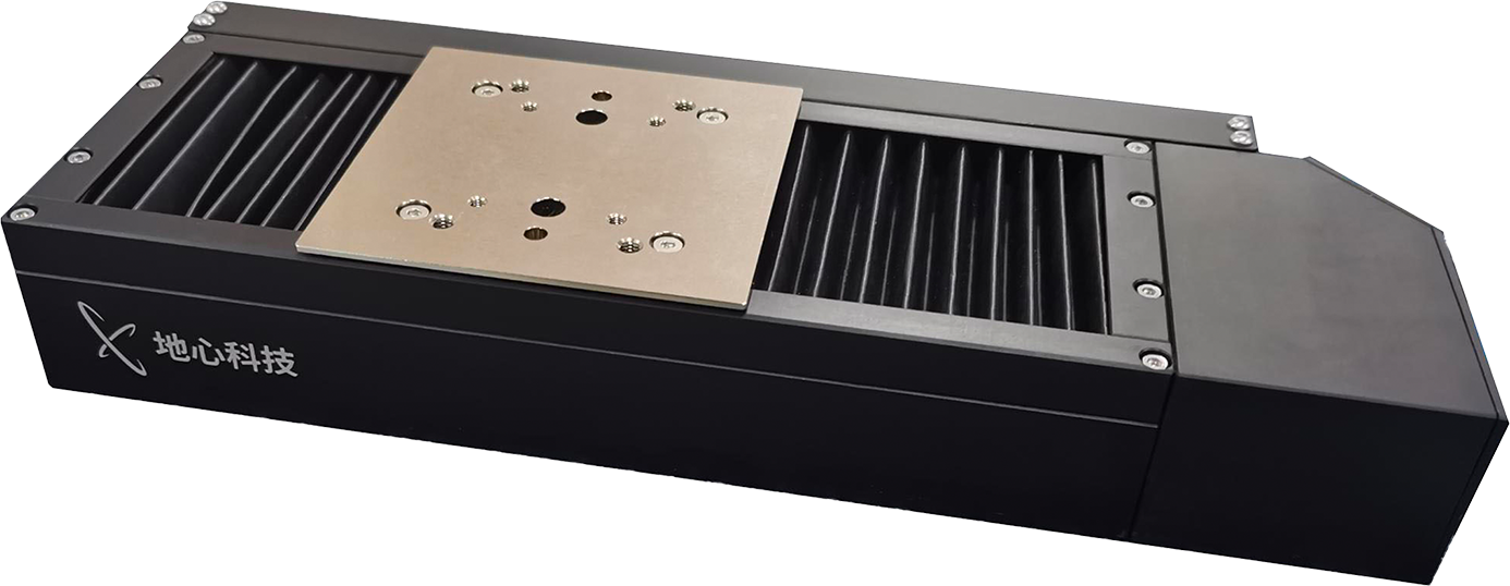
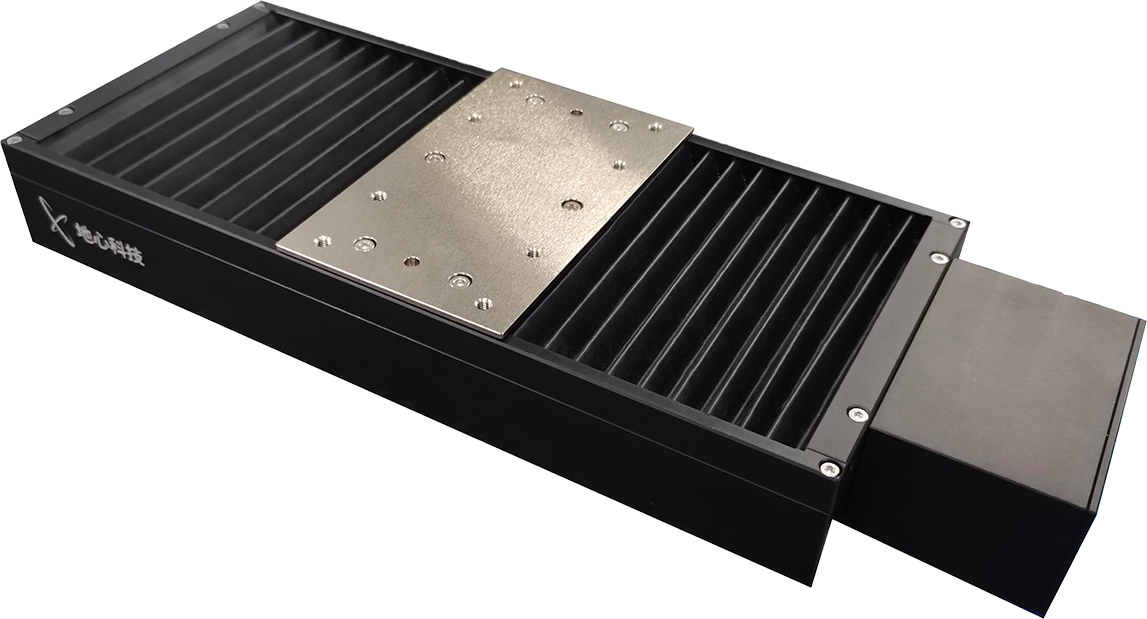
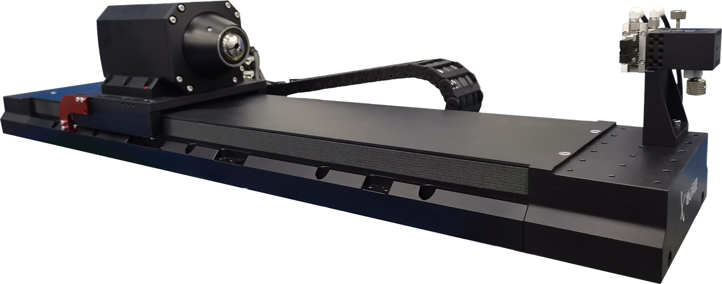
Linear axes employ air‑bearing guide technology, achieving flatness of ±0.5 μm and pitch of <2 arc sec over a 300–400 mm travel range.
The rotary stage achieves dynamic balancing to Grade G0.4 at high rotational speeds, minimising or eliminating unbalanced forces caused by non‑uniform mass distribution in rotating components. This not only improves equipment operational efficiency and service life, but also significantly reduces disturbances to the linear axes, enabling the use of higher‑resolution sensors with smaller pixel sizes.
Airflow Optimisation Design
Targeting the special airflow disturbances caused by lightweighted chucks, aerodynamic optimisation breaks through the bottlenecks of wind noise and vibration during high‑speed rotation.
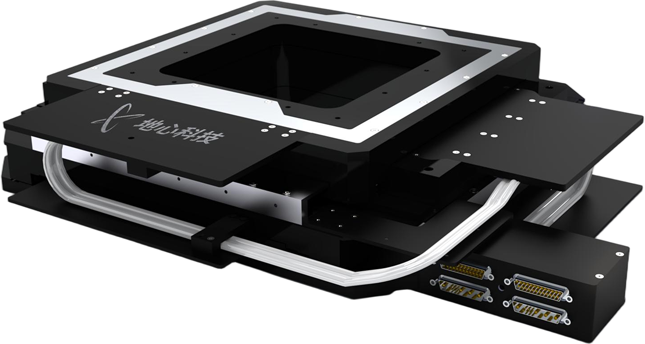
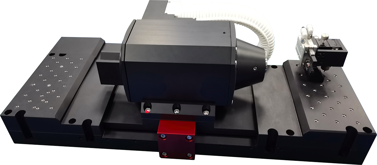
Wuxi Geocentric Technology's customised spiral inspection solution achieves wafer surface motion flatness of <5 μm under coordinated operation of linear axes and the rotary stage. Combined with a high‑dynamic‑response Z‑lift stage, dynamic focusing is enabled during motion. With the rotary stage carrying the chuck at high speeds of up to 6000 rpm, disturbances to the linear axes are maintained at less than ±0.5 μm.
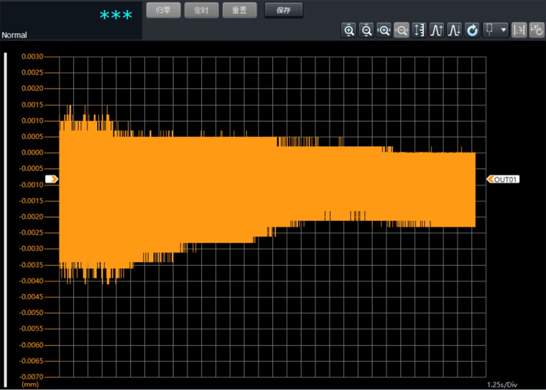
Figure 4: Wafer motion flatness <5 μm with the rotary stage carrying the chuck at 6000 rpm (Distance sensor: Keyence P015N; rotary stage speed: 6000 rpm; linear axis speed: 5 mm/s; no sampling averaging)
04 Core Products
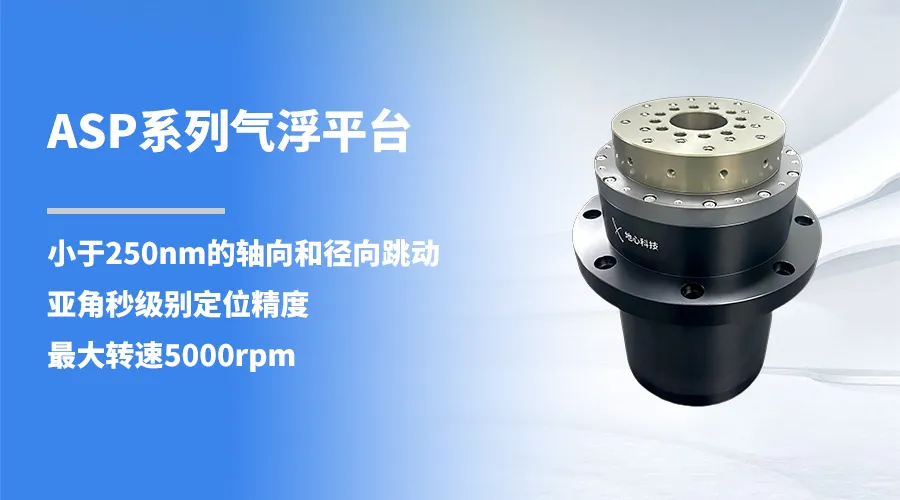
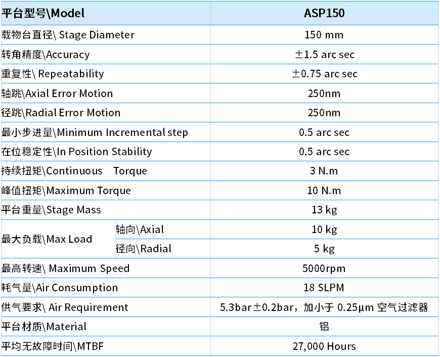
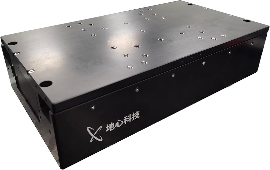
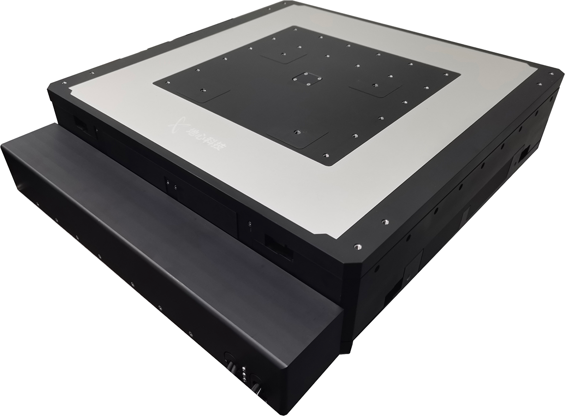
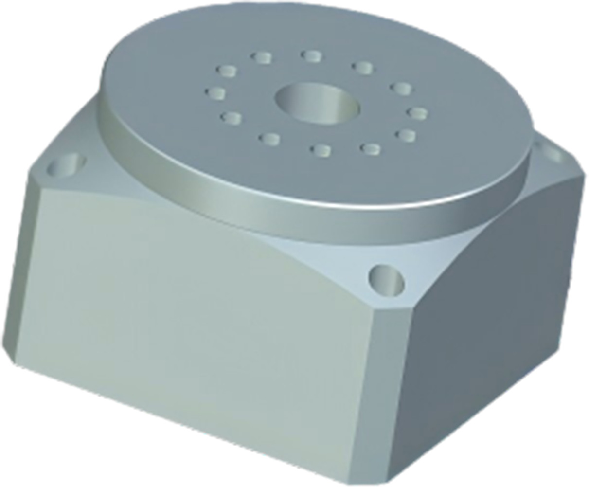
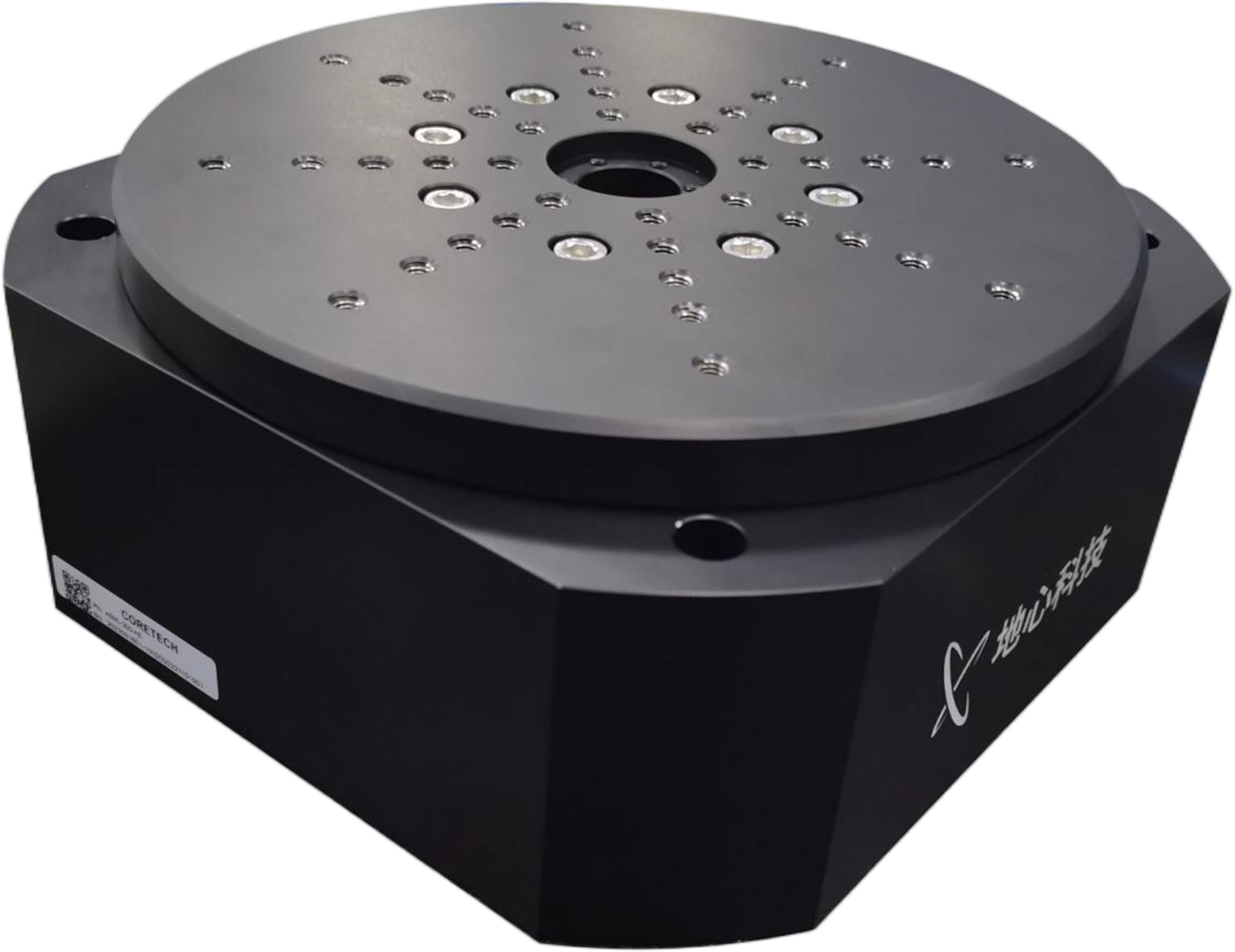
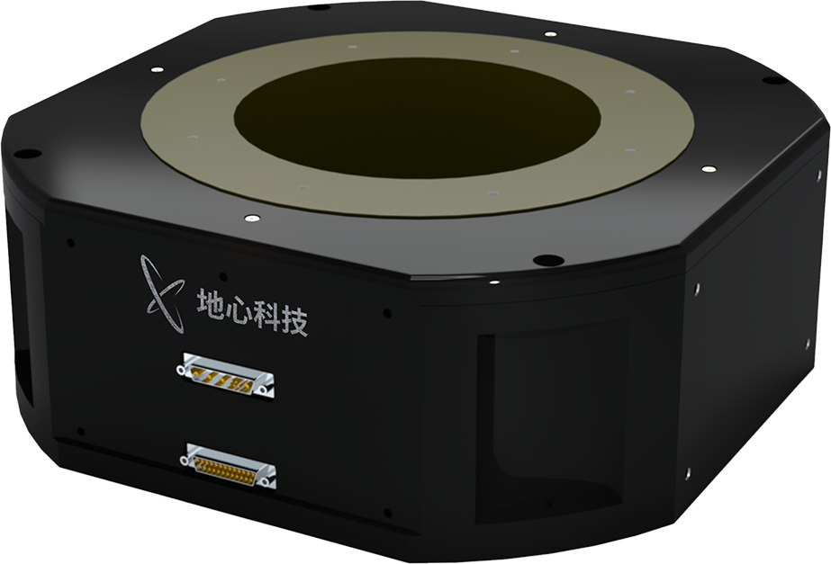
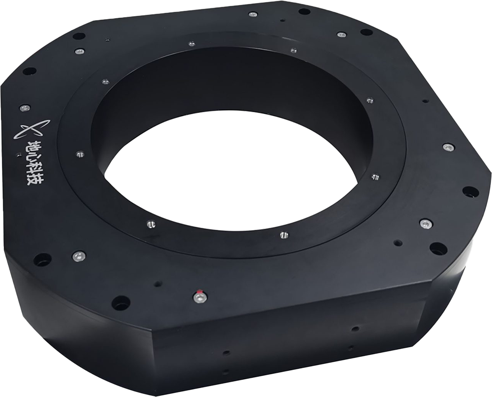
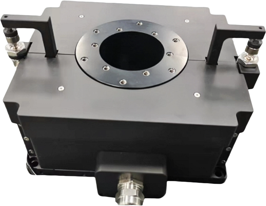
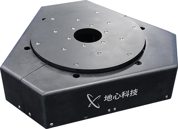
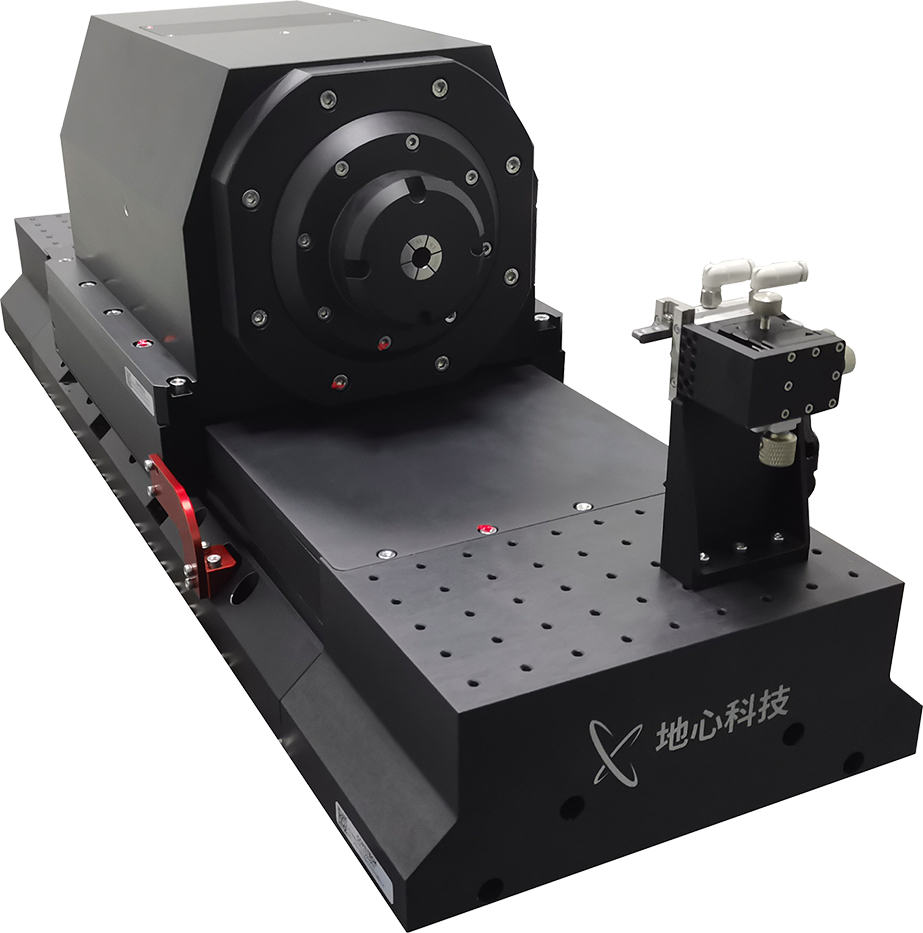
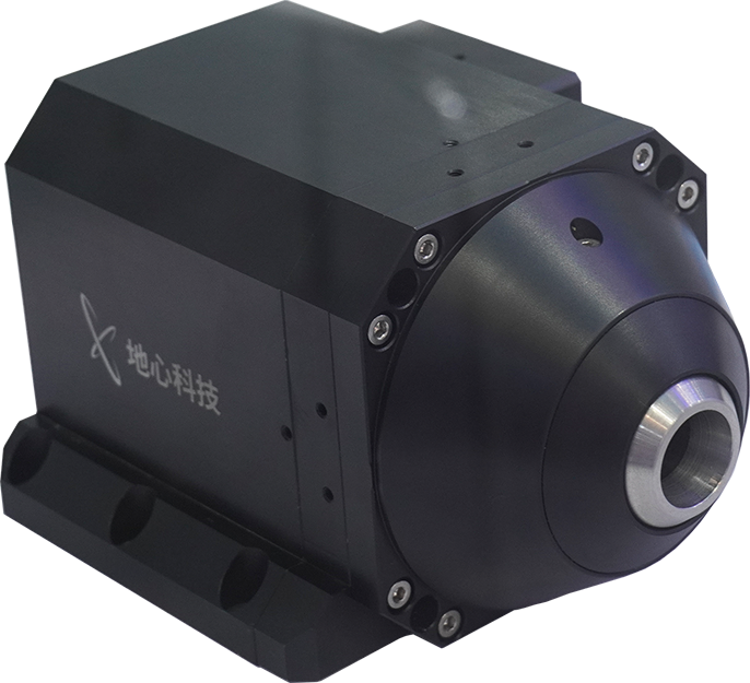
The ASP Series High‑Precision Air‑Bearing Direct‑Drive Rotary Stage employs a direct‑drive rotary motor, delivering outstanding dynamic performance and positioning accuracy. In addition to industry‑leading axial, radial, and tilt error motion characteristics, the ASP air‑bearing rotary stage offers excellent absolute rotary positioning accuracy, repeatability, and load capacity, and can be easily integrated into multi‑axis motion systems.
Specifically designed for front‑end semiconductor wafer inspection systems, it features extremely high rotational speeds and is compatible with 4.5‑inch, 6‑inch, and 9‑inch full‑size wafer processing requirements, eliminating inspection blind spots caused by travel limitations in conventional platforms.
The product supports inspection at the 5 nm process node, significantly improving wafer surface defect inspection efficiency and measurement accuracy through high‑speed dynamic response capability and nanometre‑level rotary accuracy.
Excellent positioning performance, speed stability, and high‑resolution feedback.
Non‑contact air bearings contribute to ultra‑precise motion performance.
The semiconductor wafer inspection industry is at a critical stage of technological iteration. Wuxi Geocentric Technology's spiral‑motion inspection solution, centred around air‑bearing rotary stages and combined with innovative spiral scanning, supports the self‑reliance and controllability of China's semiconductor industry chain, providing the industry with an efficient, high‑precision domestically produced solution.
This technological breakthrough not only aligns with the semiconductor manufacturing industry's core pursuit of "higher precision and lower cost," but also drives the increasing penetration of domestic equipment in the high‑end market, significantly enhancing the competitiveness of Chinese‑made equipment in the premium segment.
Featured News
Laser Processing Automation Solutions – 3D Spatial Drilling
2026.06.03
[Exhibition News] Riding the Wave of Precision Motion Control Once Again – Ground Motion Technology Makes a Stunning Appearance at Laser World of Photonics China!
2026.03.23
Laser Processing Automation Solutions – PCB Drilling
2026.06.03
 Back to List