

.png)

.png)







Home
 News Center
In Micro/Nano Direct-Write Lithography Systems, the Stage's Exceptional Dynamic Performance Enhances Lithography Accuracy and Efficiency
News Center
In Micro/Nano Direct-Write Lithography Systems, the Stage's Exceptional Dynamic Performance Enhances Lithography Accuracy and Efficiency
News Center
In Micro/Nano Direct-Write Lithography Systems, the Stage's Exceptional Dynamic Performance Enhances Lithography Accuracy and Efficiency
In Micro/Nano Direct-Write Lithography Systems, the Stage's Exceptional Dynamic Performance Enhances Lithography Accuracy and Efficiency
 2026-06-03
Share:


"Coretech's CFT series high-speed, high-precision XY integrated precision motion stage, with its outstanding dynamic performance, perfectly addresses the challenges of high-speed, high-precision alignment in micro/nano direct-write lithography applications, and is widely used in pan-semiconductor direct-write lithography equipment."
01 Direct-Write Lithography Technology
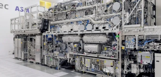
In the semiconductor field, current lithography equipment for IC and FPD manufacturing is predominantly mask-based lithography systems. The EUV lithography systems we frequently hear about are mask-based lithography tools. According to media reports, ASML has stated that a single High-NA EUV lithography system will be priced at up to USD 380 million—more than double the price of current EUV systems (approximately USD 183 million).
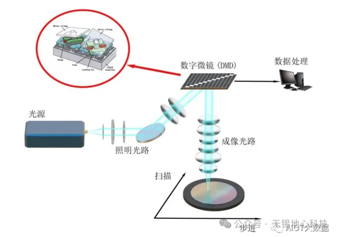
Direct-write lithography technology, also known as a pattern generator in English, is a means of generating micro/nano patterns, converting computer-designed GDSII, DXF, and other graphic files into physical layout patterns. Direct-write lithography is a maskless lithography technique. By simply controlling light intensity and scanning writing paths, it achieves high-precision writing of arbitrary patterns. Compared with other writing methods, it is simpler and more cost-effective, enabling high-precision, high-flexibility, and low-cost production.
Direct-write lithography employs high-speed real-time dynamic area-scanning writing technology. It uses high-power UV lasers or LED light sources, combined with efficient light-collection and homogenisation systems, to illuminate a digital micromirror device (DMD). Dynamic patterns are generated in real time through the data link, and these patterns are then projected directly onto a photosensitive material-coated substrate through high-precision, low-distortion projection exposure lenses. This enables simultaneous scanning exposure with millions of light beams, efficiently forming exposure patterns in real time through spatial area scanning and seamless stitching technology.
02 Key Aspects of Micro/Nano Direct-Write Lithography Technology
Direct-write lithography and projection lithography are two distinct classes of lithography technologies with clearly defined roles in the current industry. In lithography applications involving substrate warpage or substrate deformation—such as Fan-Out, COF, and other advanced packaging developments—packaging lithography technology requires smaller line widths, larger format sizes, and enhanced pattern alignment and overlay adaptation capabilities. The adaptive adjustment capability of direct-write lithography provides advantages such as high yield and excellent consistency.
The key technical challenges faced by direct-write lithography equipment not only include lithography light sources and line-width quality, but also encompass technical issues unique to direct-write lithography: high-speed, high-precision motion stages and position accuracy; pattern stitching; and large-volume pattern data generation along with high-speed, real-time, distortion-free data transmission—all of which are critical points in equipment integration and manufacturing.
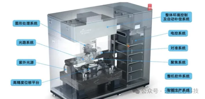
The high-precision, wide-dynamic-range lithographic optical imaging system projects patterns reflected by the digital micromirror device through optical lenses with high precision onto the photosensitive material-coated substrate. This system is one of the critical modules of lithography equipment. It must not only have a sufficiently large numerical aperture to ensure resolution that meets line-width accuracy requirements, but also maintain image quality close to the ideal, with distortion controlled within 0.001%. To ensure consistency in parallel operation of multiple imaging systems, the lens magnification needs to have a certain fine-tuning capability.
The high-precision, high-speed real-time autofocus system is another key technical aspect of the equipment, ensuring that patterns are consistently exposed at the optimal focal plane during the lithography process, thereby maintaining line-width accuracy. Due to variations in substrate thickness, differences in surface flatness, fluctuations in vacuum chuck flatness, and the limited depth of focus of the projection imaging system, each lens must be equipped with a high-precision real-time focusing system to ensure uniformity of the overall exposure effect across the substrate. This system measures substrate surface flatness differences in real time through a measurement system, and a nano-actuator adjusts the distance between the lens and the substrate to keep the substrate constantly at the optimal imaging position of the lens.
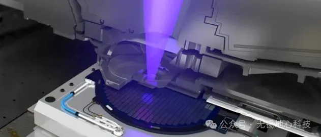
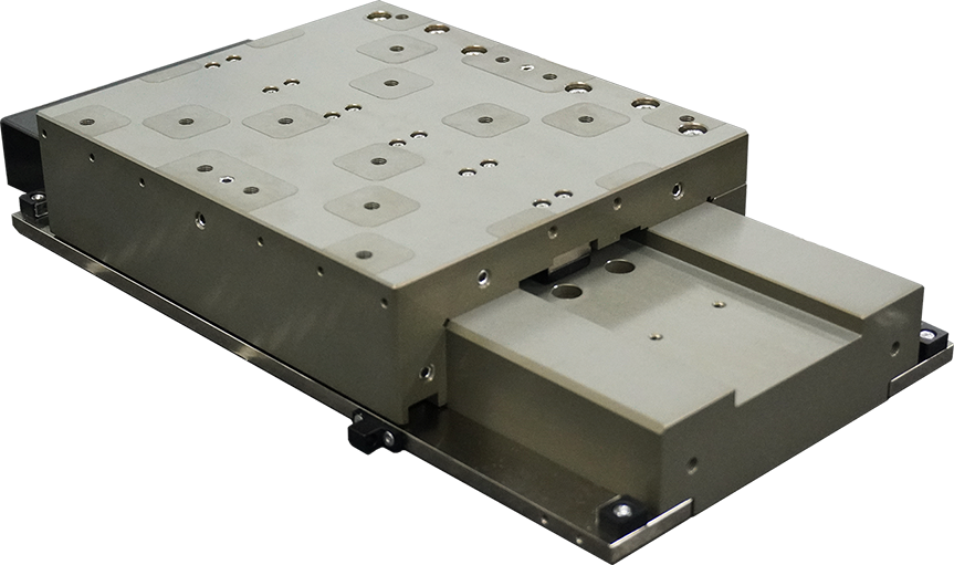
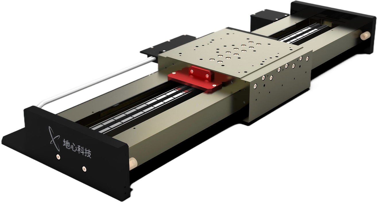
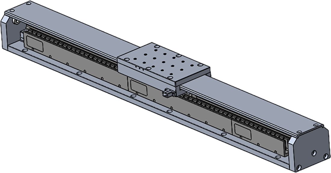
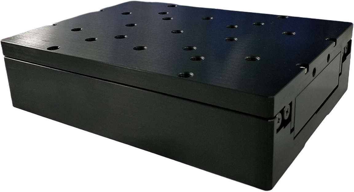
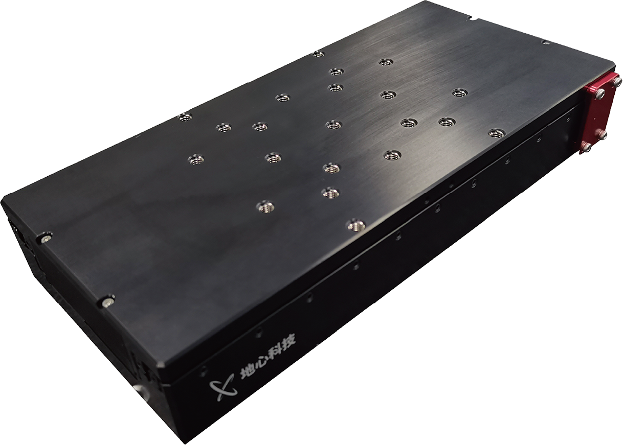
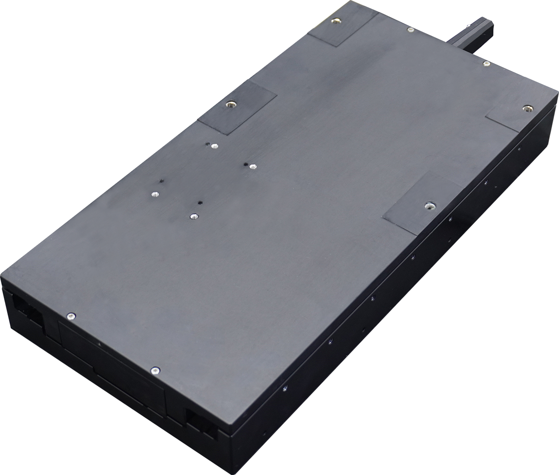
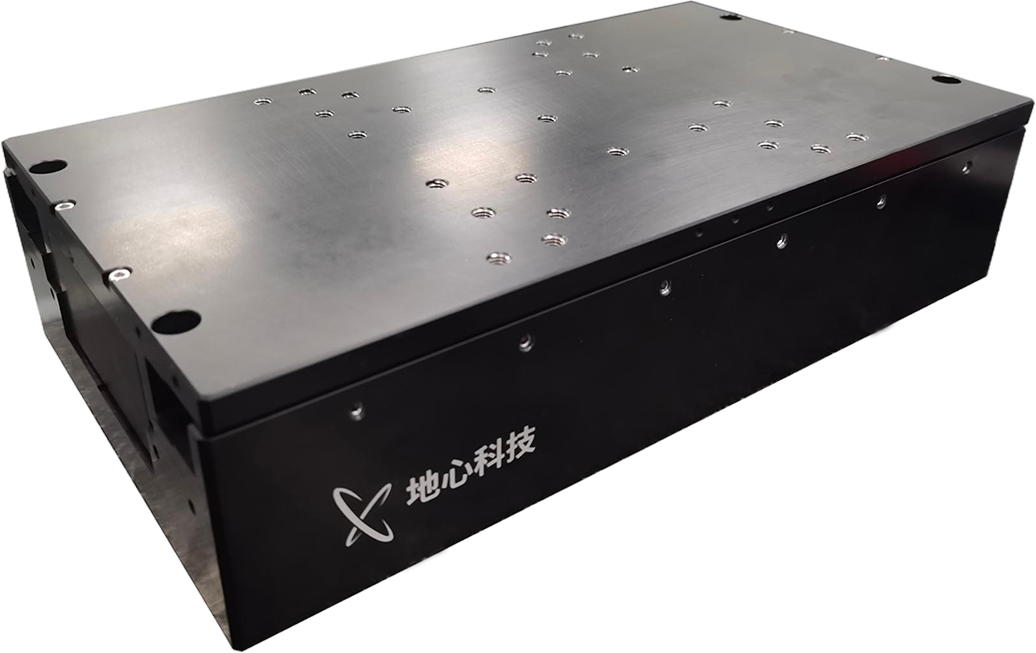
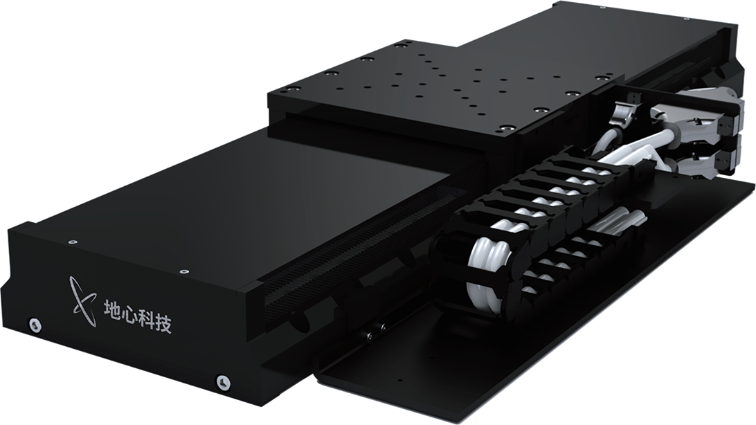
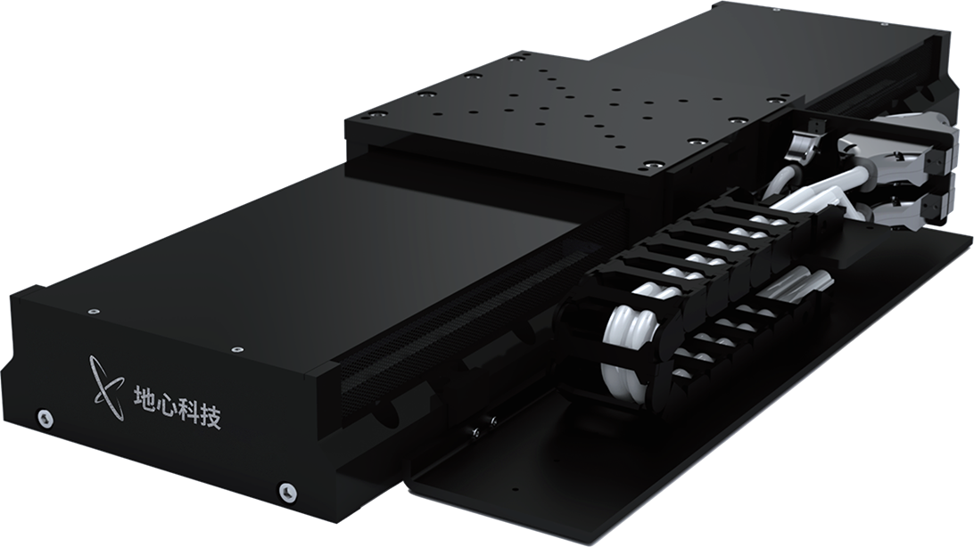
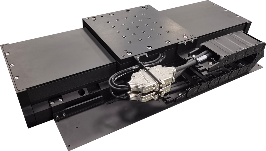
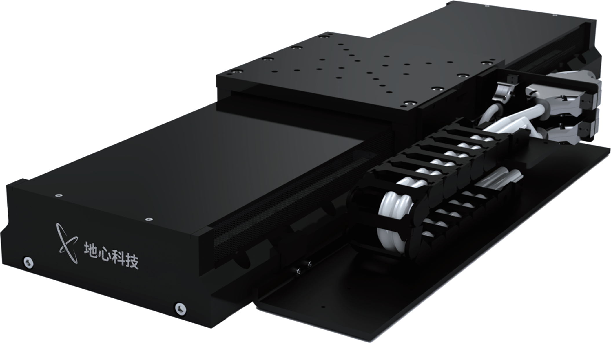
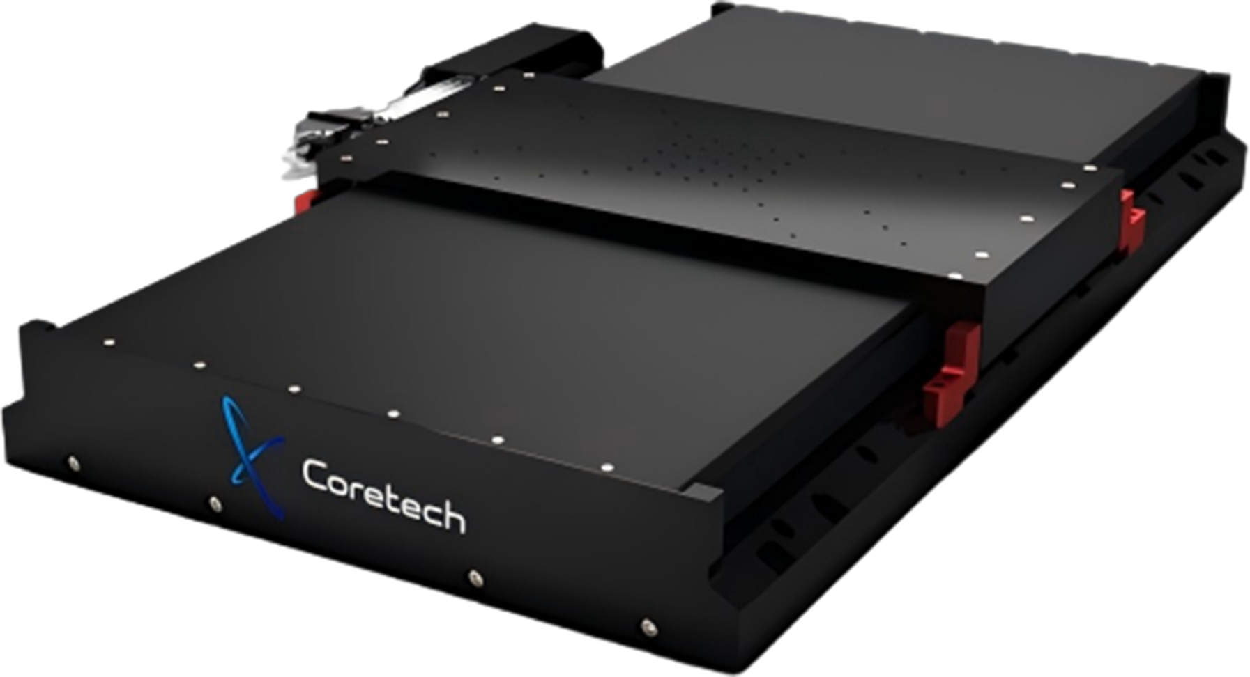
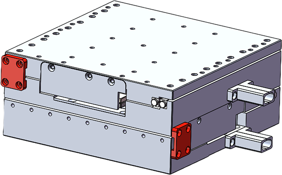
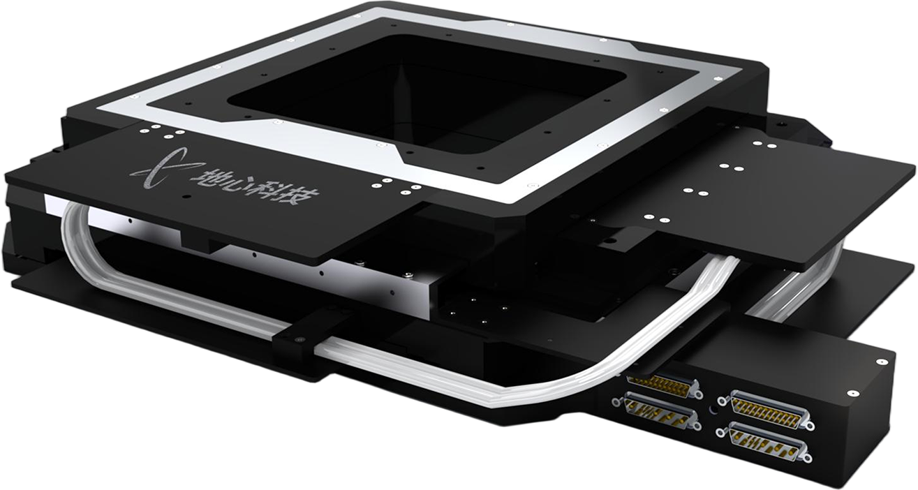
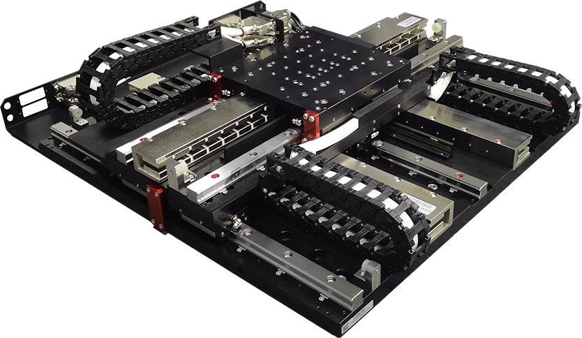
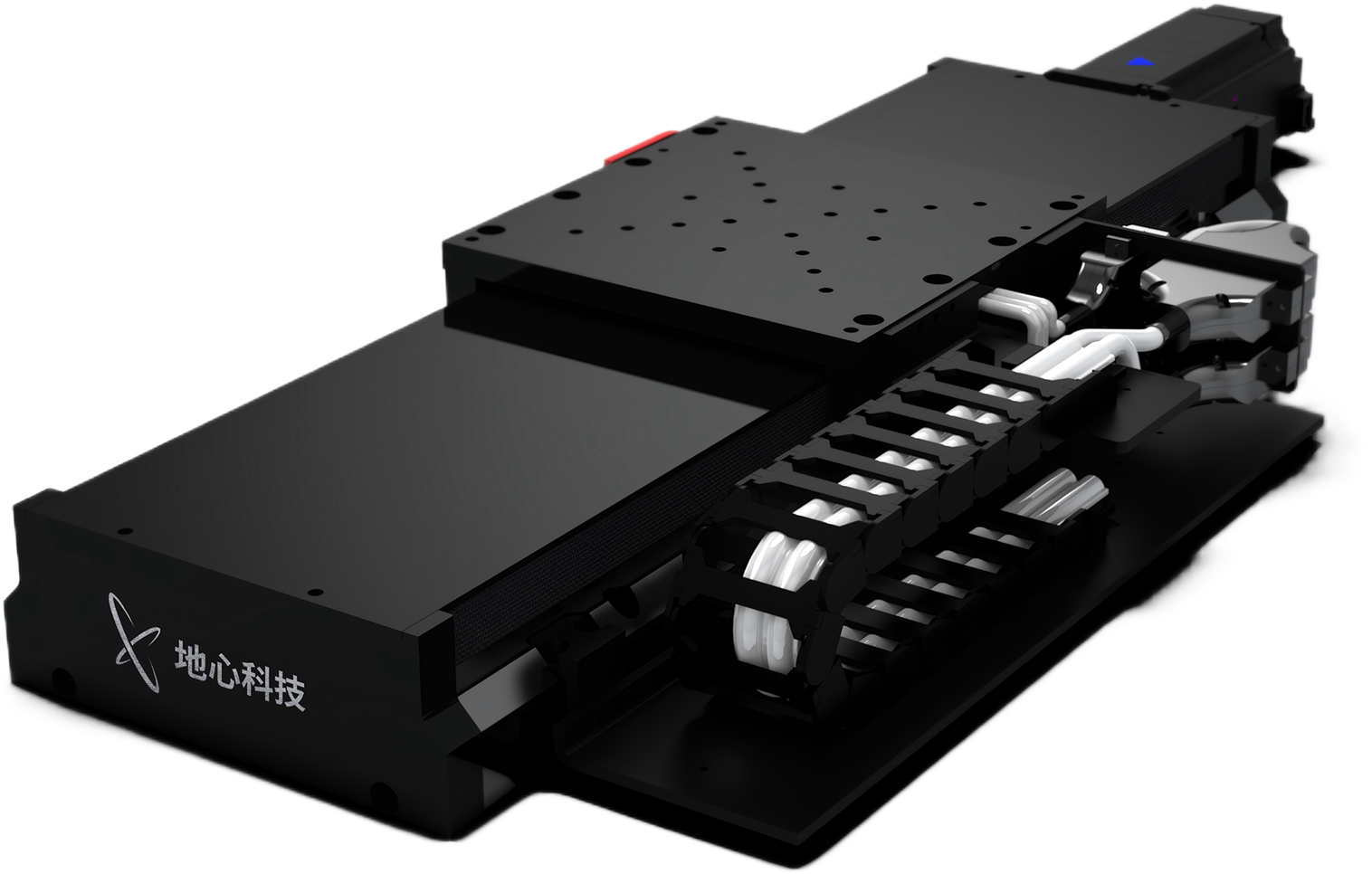
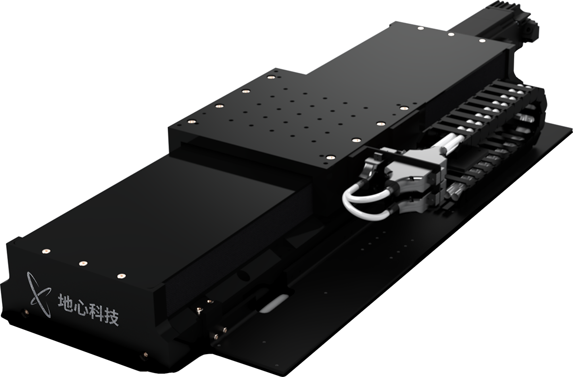
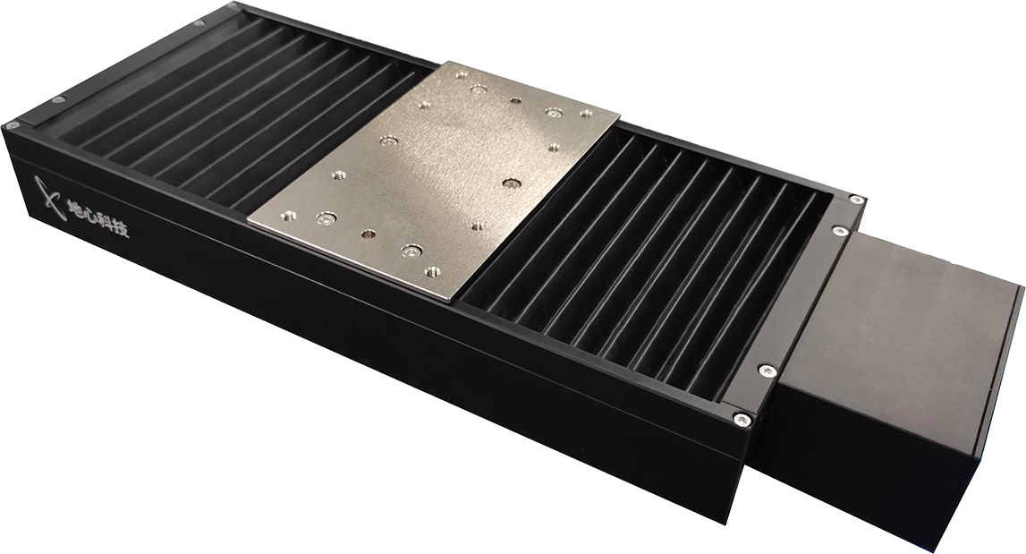
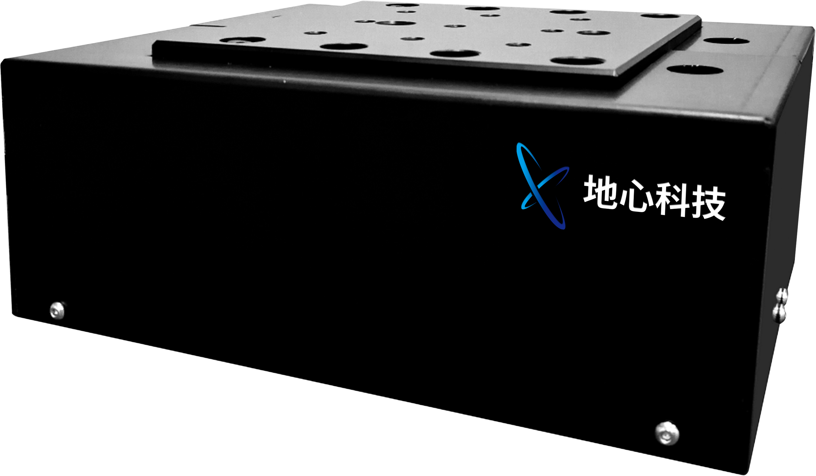
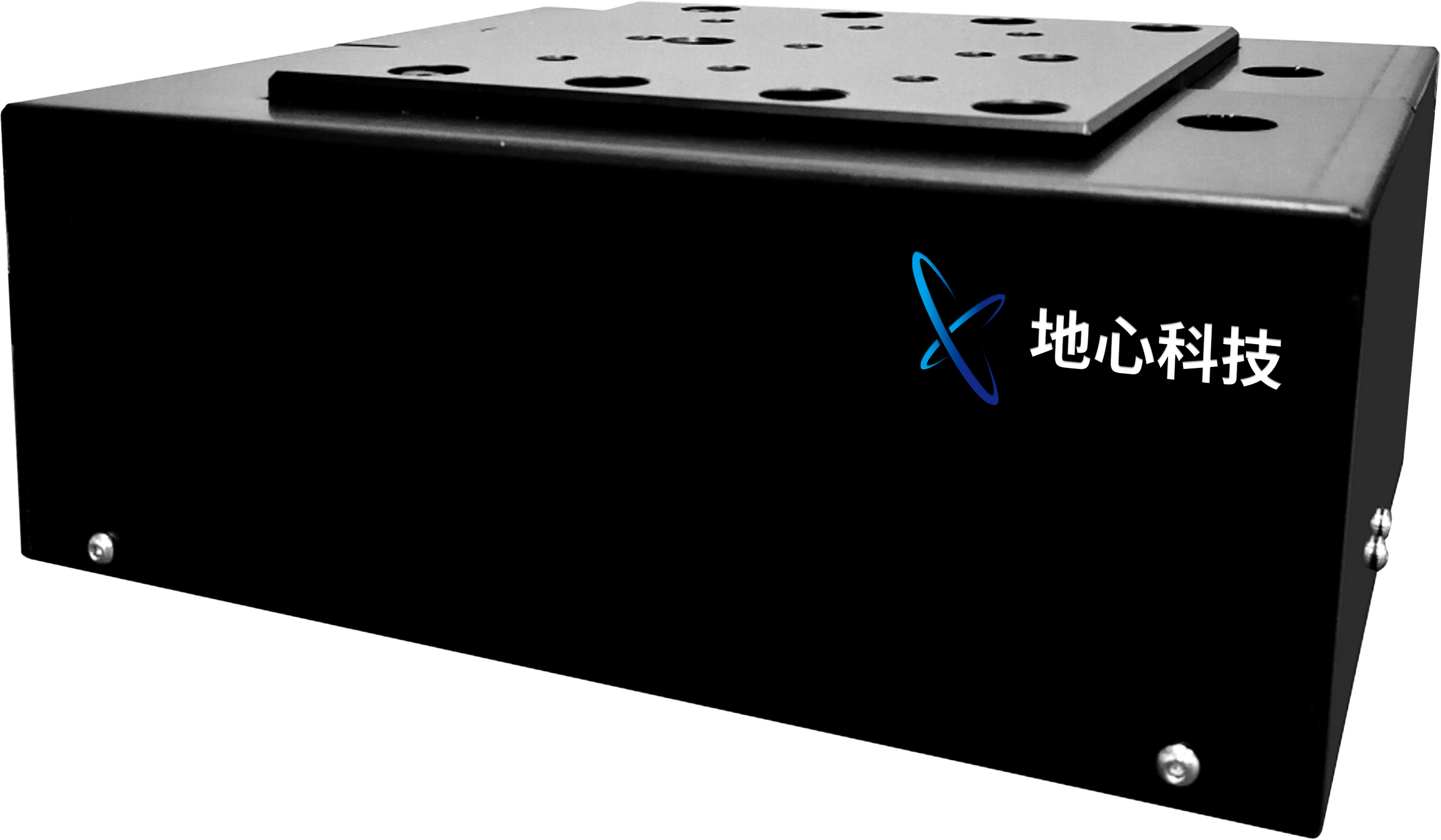
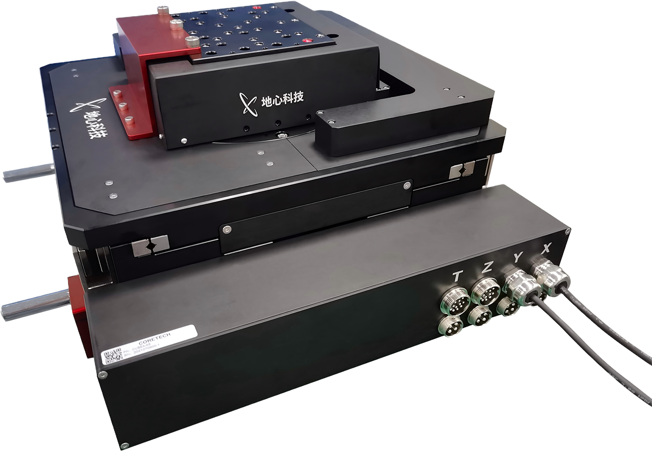
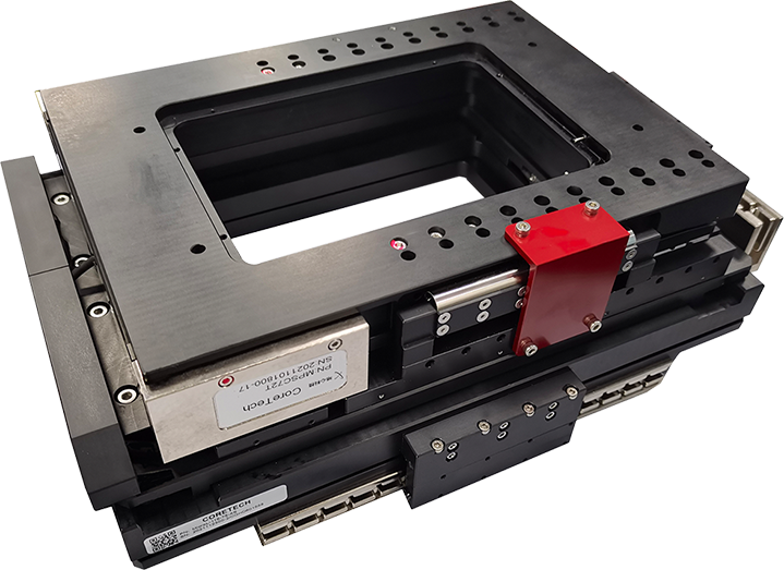
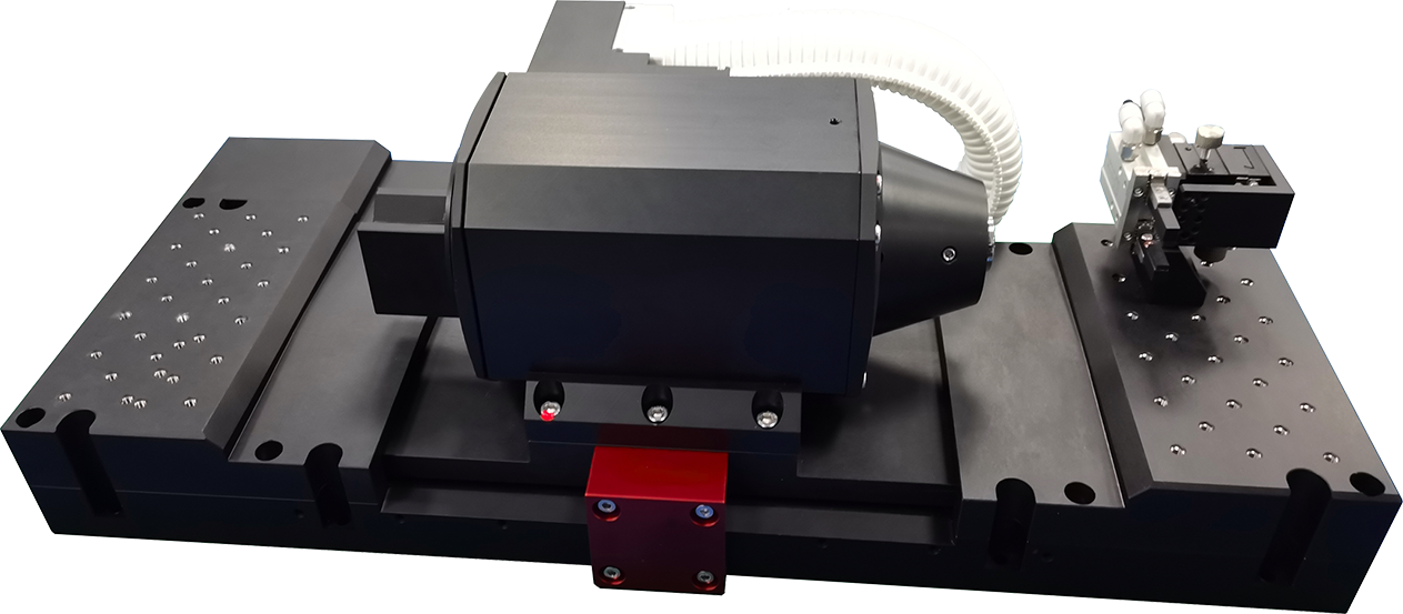
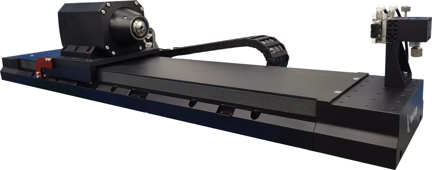
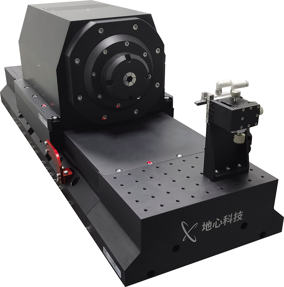
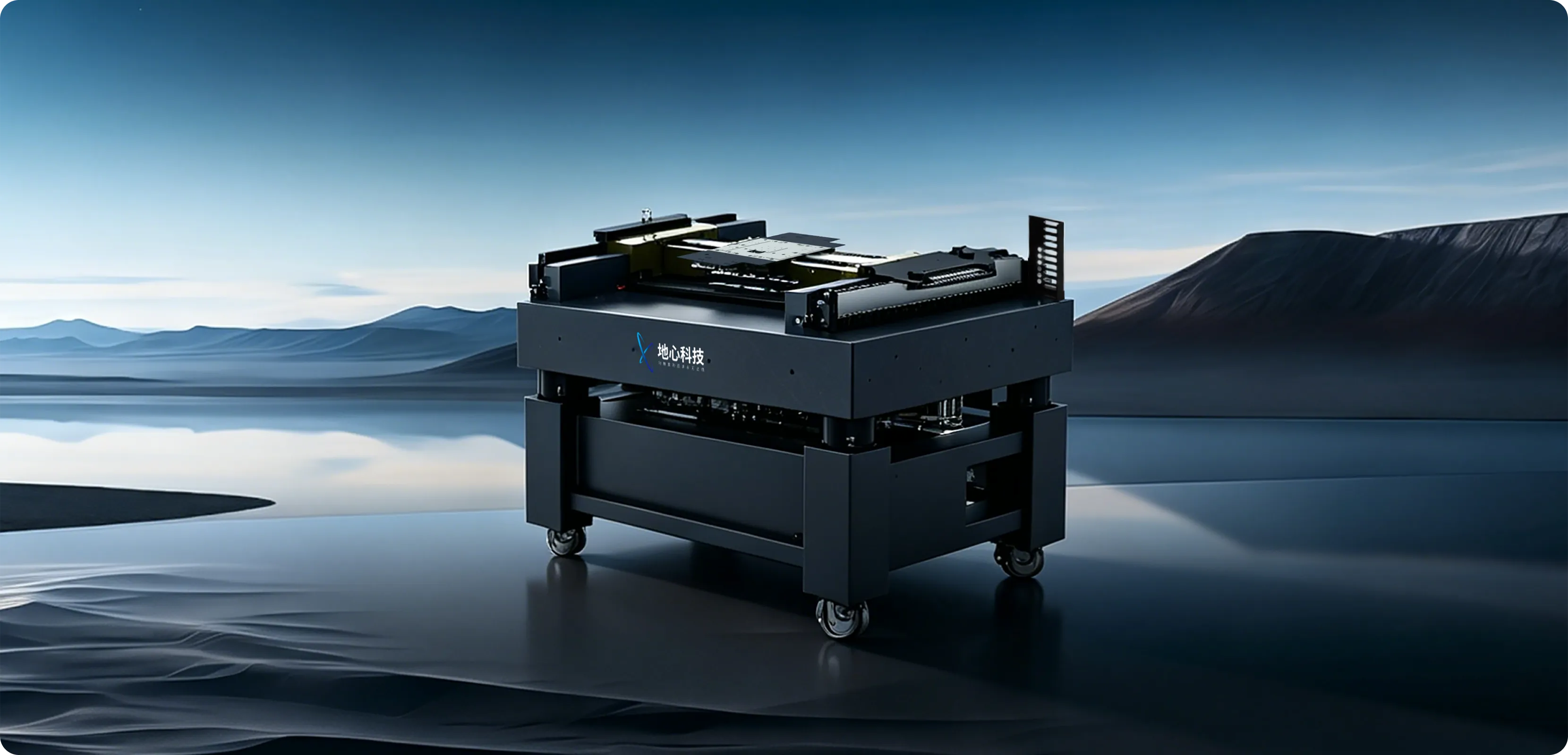
Coretech products are widely used in micro/nano direct-write lithography applications. The CFT-200XY XY integrated motion platform is a precision positioning stage with nanometre-level positioning accuracy. It features direct-drive linear motor control with dual motors per axis, and employs precision cross-roller guides for exceptional dynamic performance and positioning accuracy. Its compact structure, low lateral height, and reduced Abbe error are key advantages.
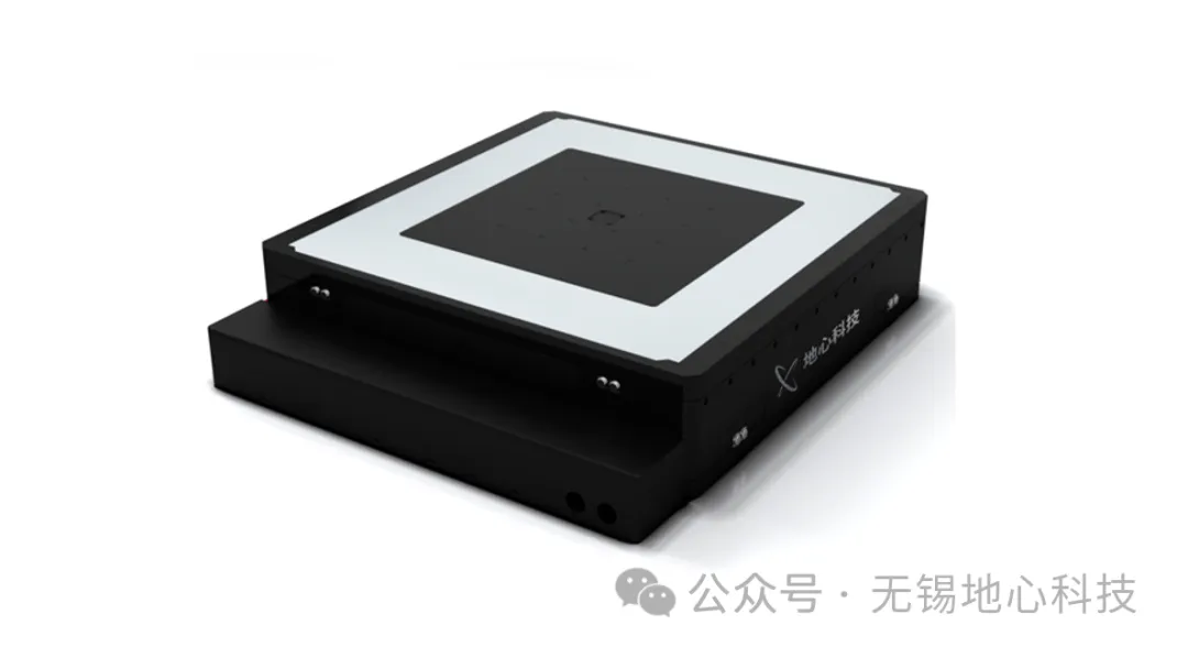
| 有效行程: | 200*200mm; |
| 双向重复定位误差: | ≤±0.1um; |
| 平面度: | ≤±1.5um; |
| 最大速度: | 800mm/s |
| 最大负载: | 20kg; |
| 最小步进量: | 5nm; |
| 在位稳定性: | ≤±3nm; |
The CFT-200XY integrated motion platform achieves straightness within ±2 μm over 300 mm, resolution of 1 nm, repeatability of ±100 nm, and positioning accuracy of ±400 nm. The stepping axis achieves in-position stability of 3 nm (configured with ASH feedback option and linear amplifier). Multiple feedback options are available, including AS, ASH, and TTL. The CFT series is available in travel options of 200 mm × 200 mm and 300 mm × 300 mm.
04 Test Results
Coretech's classic solution—the CFT-200XY XY integrated motion platform—has been extensively used and validated in the inspection systems of many partners.
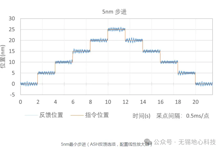
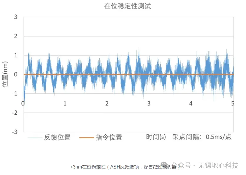
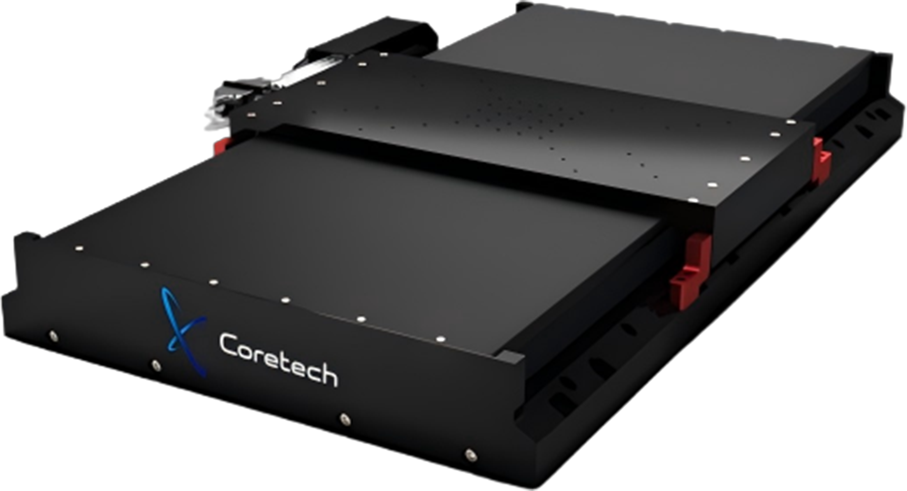
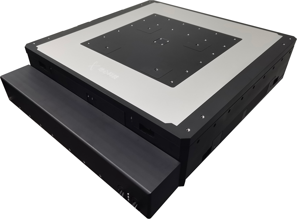
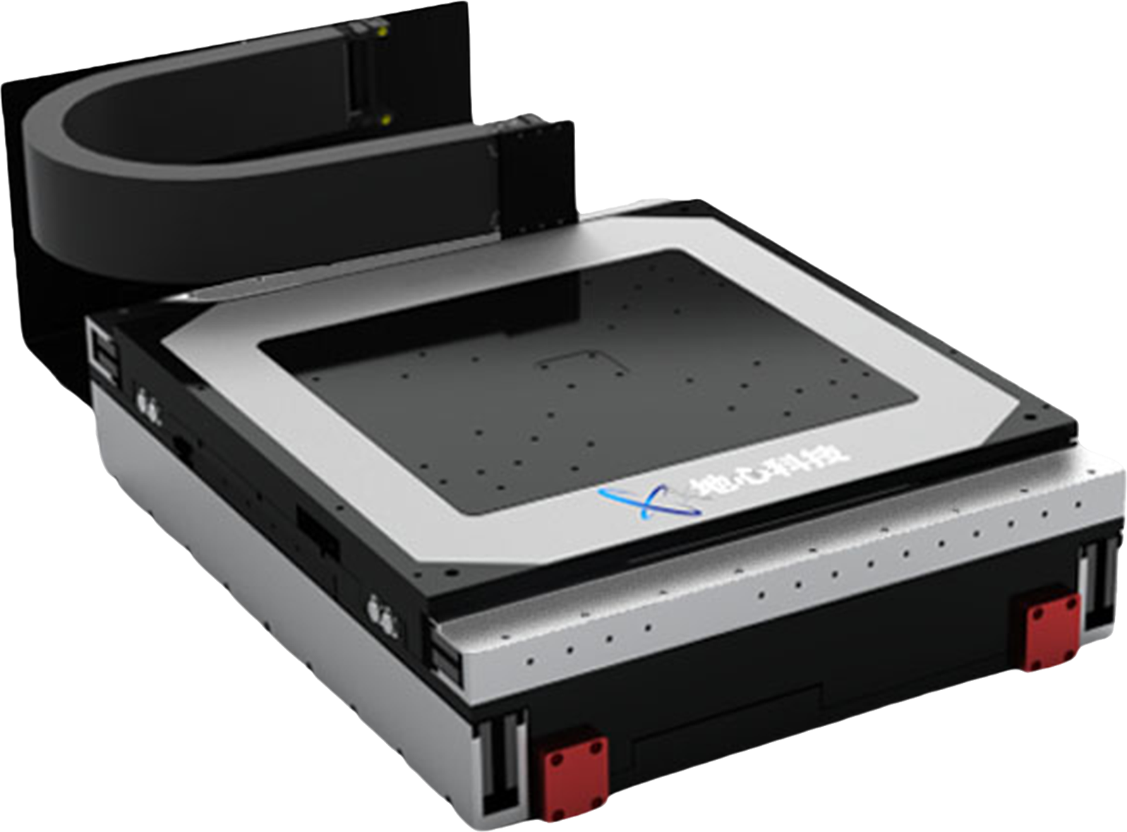
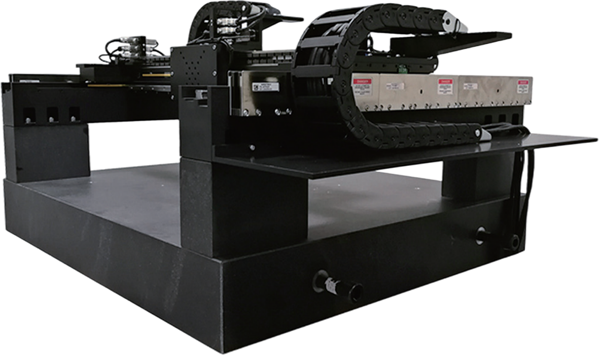
In addition to the classic CFT-200XY XY integrated motion platform, Coretech also offers the higher-end Surface series planar air-bearing stages, which are frequently used in direct-write lithography applications.
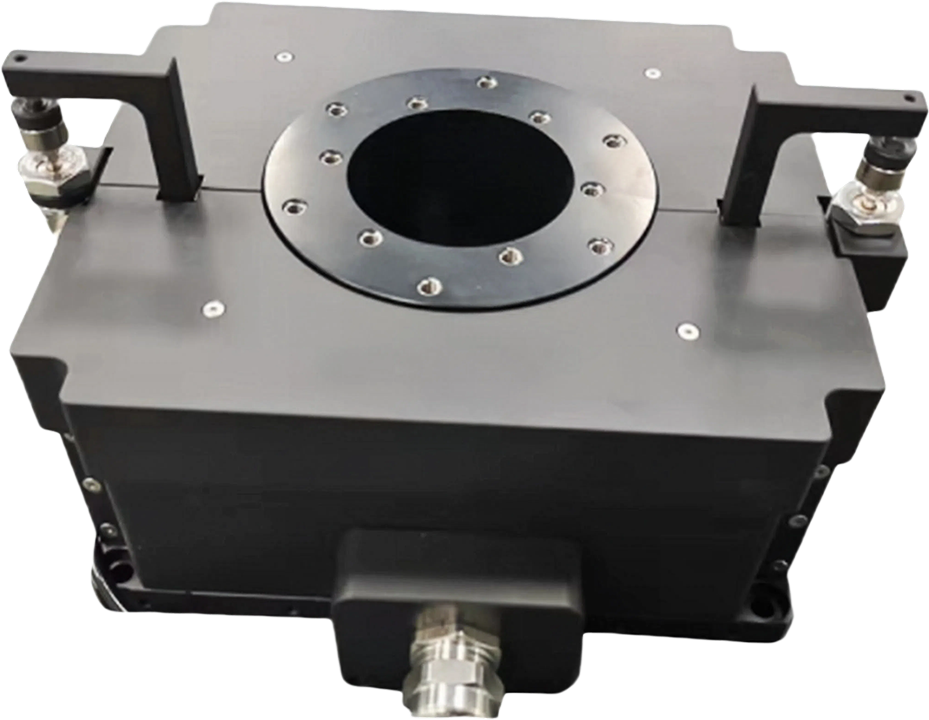
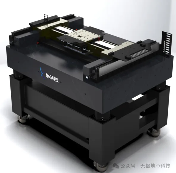
The Surface series is Coretech's high-precision, high-dynamic-performance planar air-bearing stage. It features an XY dual air-bearing positive/negative pressure design with air-cushion preloading, using negative air pressure to balance the upward floatation and downward preload forces of the air-bearing guides, ensuring proper air gap clearance. Its geometric performance is exceptional, with an effective travel of 350 mm × 350 mm. Pitch and yaw angles are both less than 2 arc seconds, with resolution of 1 nm, repeatability of ±100 nm, and positioning accuracy of ±250 nm. Maximum speed reaches 2 m/s, and maximum acceleration is 2 g.
Featured News
High-Precision Motion Stages Enhancing Coupling Alignment Accuracy in Precision Fiber Coupling Equipment
2026.06.03
Behind the Mass Production of Hybrid Bonding: How Precision Motion Stages Meet the High-Precision Control Demands of Semiconductor Packaging
2026.06.02
Improving Yield and Efficiency: High‑Precision Motion Stages Empowering Innovation in Laser Direct Writing Technology
2026.06.03
 Back to List