

.png)

.png)







Home
 News Center
From Optical Chip Manufacturing to Fiber Coupling: Ultra‑Precision Motion Control Platforms Enabling a Technological Leap in the Optical Communications Industry
News Center
From Optical Chip Manufacturing to Fiber Coupling: Ultra‑Precision Motion Control Platforms Enabling a Technological Leap in the Optical Communications Industry
News Center
From Optical Chip Manufacturing to Fiber Coupling: Ultra‑Precision Motion Control Platforms Enabling a Technological Leap in the Optical Communications Industry
From Optical Chip Manufacturing to Fiber Coupling: Ultra‑Precision Motion Control Platforms Enabling a Technological Leap in the Optical Communications Industry
 2026-06-03
Share:


We live in an era enveloped by data.
From artificial intelligence to 5G high‑definition video and the countless smart devices of the Internet of Things, massive amounts of information surge across the globe like tidal waves. Underpinning all of this is an invisible super‑highway – the optical communication network. It travels at the speed of light, interconnecting the world and serving as the neural network of modern civilisation. Yet behind this information artery, an extreme race of speed and precision is quietly unfolding.
01 Optical Communications: The Invisible Artery of the Digital World
Compared with traditional electrical communications, optical communications offer incomparable advantages.
First is the enormous transmission bandwidth. Theoretically, a single optical fibre offers almost unlimited bandwidth. Using technologies such as wavelength‑division multiplexing (WDM), hundreds or even thousands of signals can be transmitted simultaneously over one fibre, easily achieving terabit‑per‑second transmission rates. Second are the extremely low transmission losses and high fidelity – optical signals propagating through specially designed fibres suffer minimal attenuation, ensuring information integrity over long‑distance transmission.
Driven strongly by demands from 5G, cloud computing, the Internet of Things, and artificial intelligence, global data traffic is growing exponentially, and the optical communications industry is therefore facing unprecedented development opportunities.
02 Precision Wins: The Cornerstone of High‑Speed Optical Communications
The optical communications industry chain comprises upstream, midstream, and downstream segments. The upstream primarily includes core components such as optical chips, optical sub‑assemblies, and electrical chips; the midstream includes optical devices, optical modules, and optical communications equipment; and the downstream is divided by application scenarios into telecom and data‑com markets.
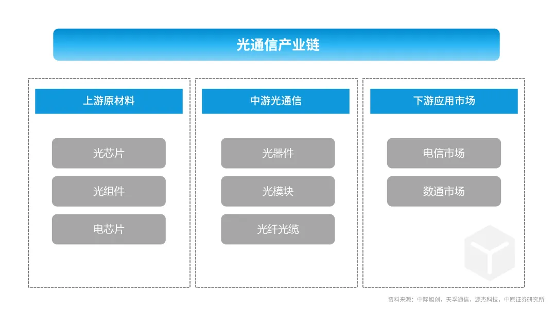
Figure 2: Overview of China’s optical communications industry chain
Optical chips are one of the core elements of the optical communications industry chain.
At the transmitting end, laser chips perform electro‑optic conversion, transforming electrical signals into optical signals, which are then transmitted through optical fibres to the receiving end, where detector chips perform opto‑electric conversion, converting optical signals back into electrical signals. In network systems such as fibre‑to‑the‑x (FTTx), 4G/5G mobile communication networks, and data centres, optical chips are the key determinants of transmission speed and network reliability.
Precision motion control platforms act as the “ultra‑precision hand” running through the entire optical chip manufacturing chain. Their technological breakthroughs directly drive improvements in optical chip integration density and performance while significantly reducing production costs.
The core structures of optical chips typically require sub‑micrometre or even nanometre dimensions. For example, the silicon‑photonic integrated optical‑gyroscope transceiver chip developed by the Joint Micro‑Optics Center has a minimum structural width of only 0.15 μm (about 1/660 of a human hair) and integrates dozens of optical devices on a chip area of 0.2 cm².
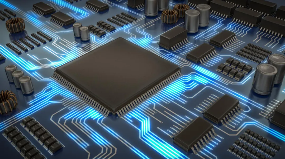
Furthermore, fibre coupling serves as the nanometre‑scale energy transfer interface between the optical fibre and the optical chip. Its alignment accuracy directly affects optical transmission efficiency – precisely aligning the external fibre with the tiny optical waveguides on the chip to enable efficient coupling of optical signals in and out.
This process is like “threading a needle” through a channel finer than a human hair. Any minute positional deviation can lead to significant signal attenuation or even complete loss, ultimately compromising the performance and reliability of the entire communication system. As optical modules evolve toward 800G and higher data rates, and as silicon‑photonics technology brings a dramatic increase in channel counts, the requirements for coupling alignment accuracy and efficiency have reached unprecedented levels.
Precision motion control platforms likewise play an irreplaceable core role in the fibre‑coupling alignment process, with their accuracy directly determining optical signal transmission efficiency and device performance. The core diameter of a single‑mode fibre is typically only 5–10 μm. To achieve efficient transmission, the end‑face positional deviation must be controlled to sub‑micrometre levels (<1 μm), and angular deviation must be less than 0.1°. For example, in the coupling and packaging of a laser diode to a single‑mode fibre, a lateral offset of 1 μm may cause a transmission efficiency drop of approximately 10%; at an offset of 2 μm, efficiency may decrease by about 30%.

All of this relies on the precise guidance of photons through micron‑ or even nanometre‑scale channels. Therefore, in the world of optical communications – especially in the manufacture of high‑speed optical modules and silicon‑photonic chips – precision is paramount.
03 Unblocking the “Manufacturing Pain Points” of the Optical Communications Industry with Precision Motion Control Technology
Precision motion control platforms play a decisive role in the optical chip fabrication process. Their accuracy and stability directly affect chip performance, yield, and production costs.
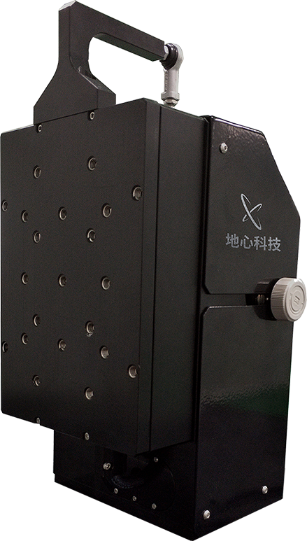
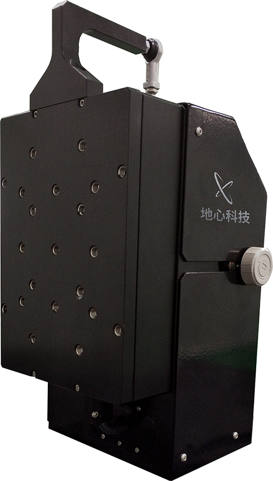
Addressing the core pain points of the optical communications industry – “difficult high‑precision alignment, difficult adaptation to multiple scenarios, and difficult efficiency improvement in mass production” – Geocentric Technology, with deep roots in the optical communications sector, delivers proven, hard‑earned solutions validated by leading industry customers.
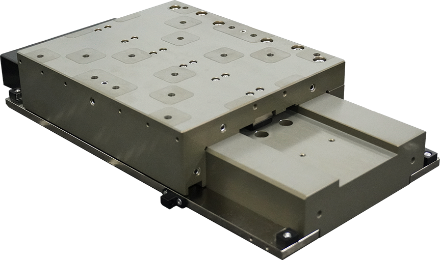
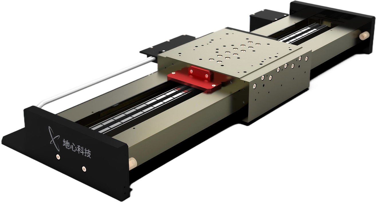
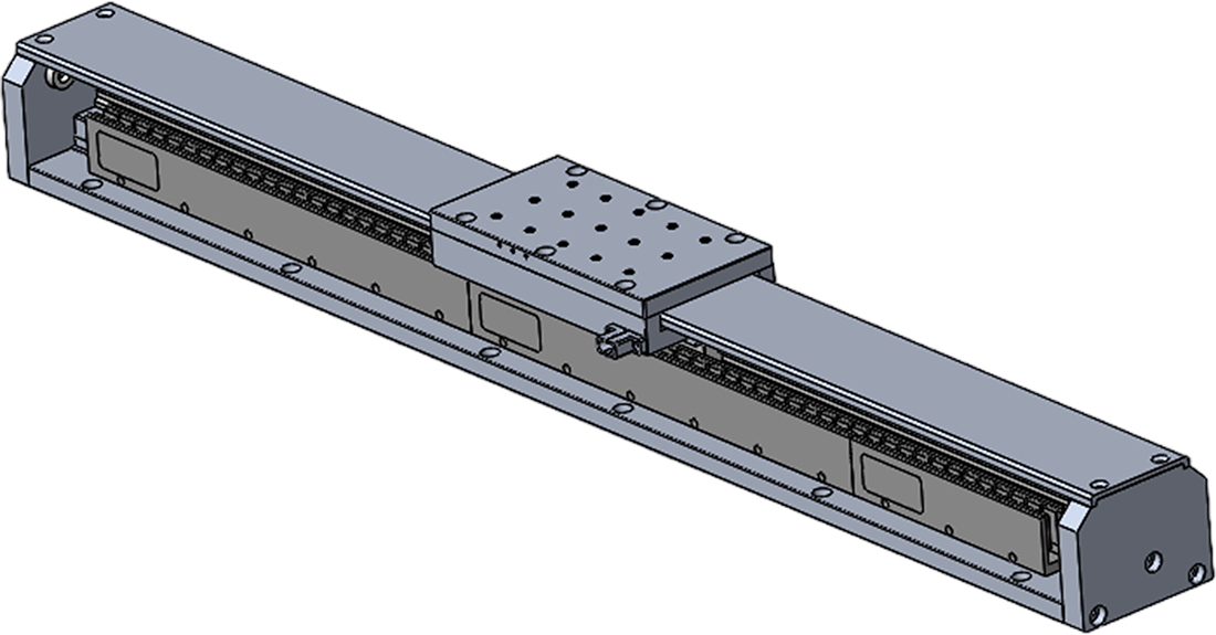
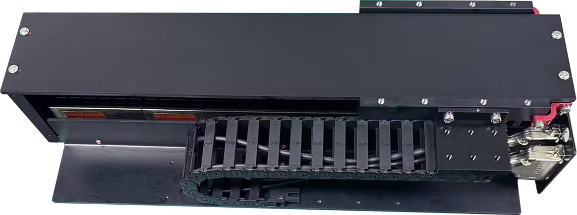
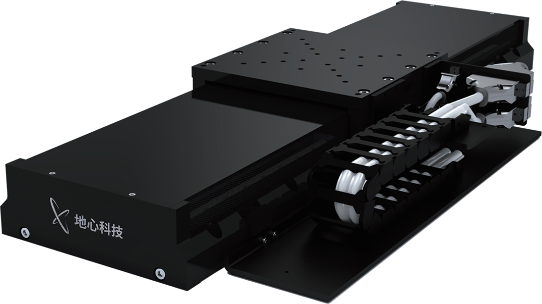
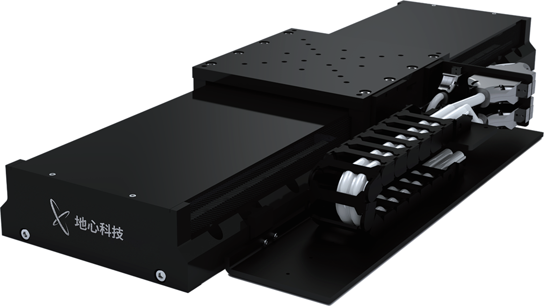
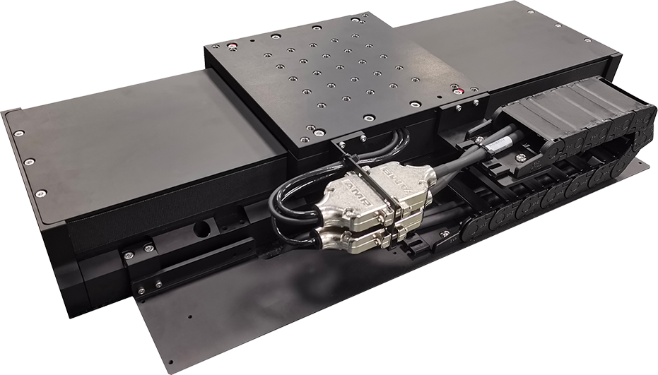
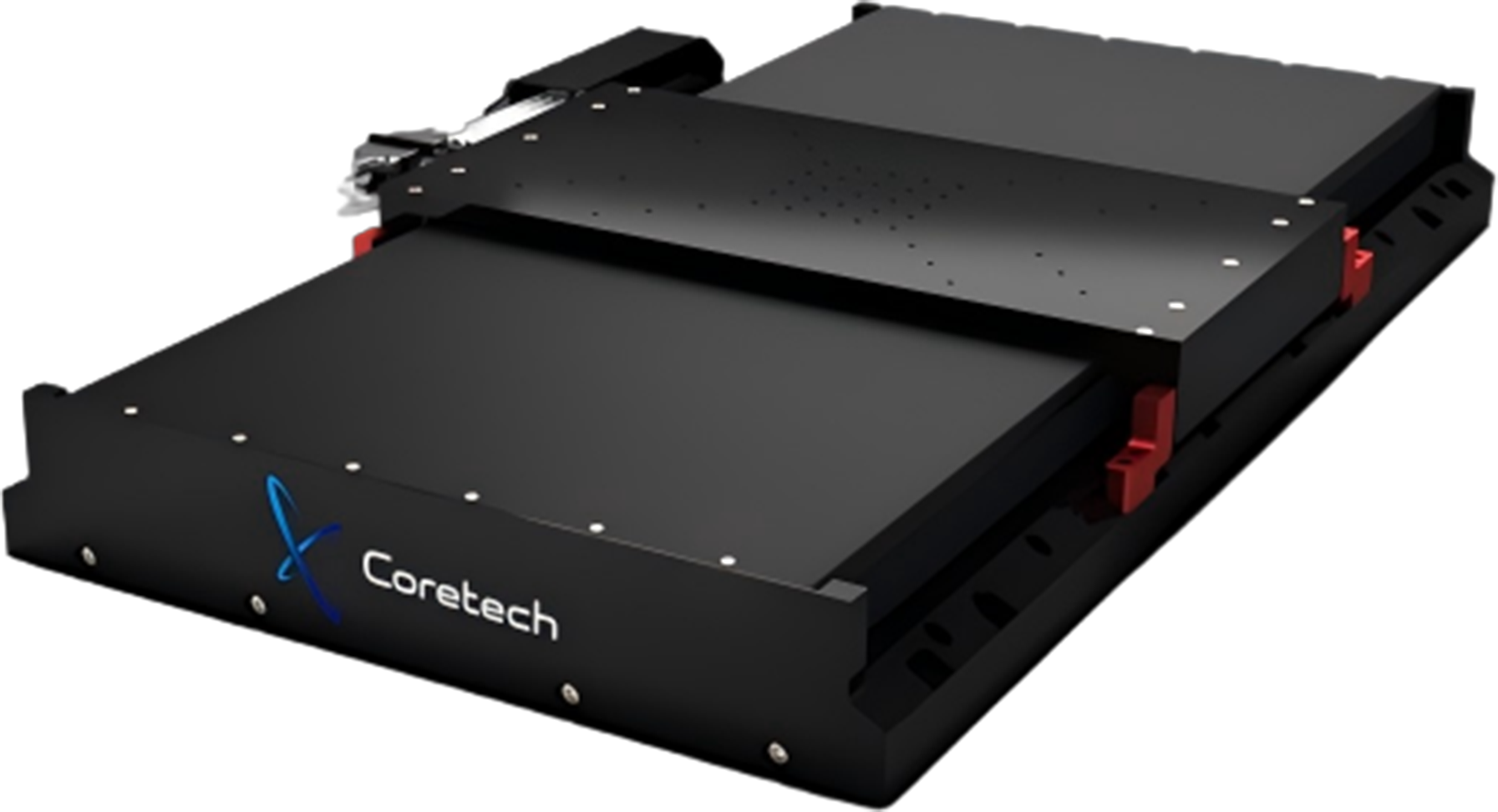
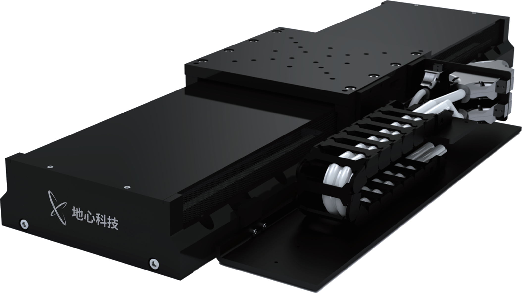
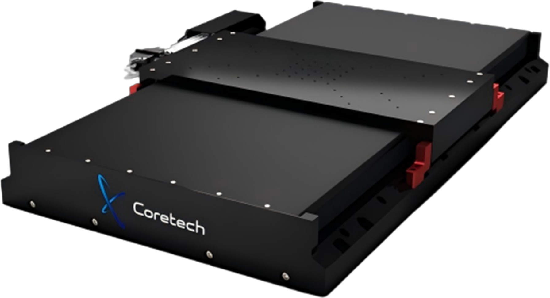
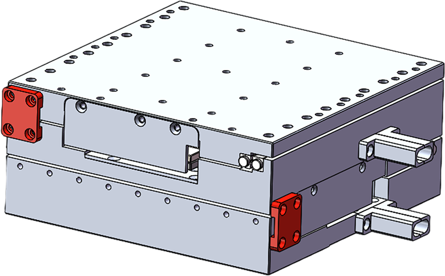
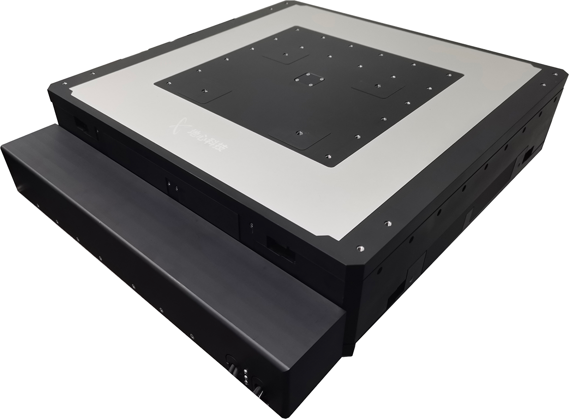
Geocentric’s product portfolio covers the entire optical communications manufacturing process, from optical chip fabrication and optical module packaging to fibre coupling, providing critical support at every stage with ultra‑high precision manipulation capabilities.
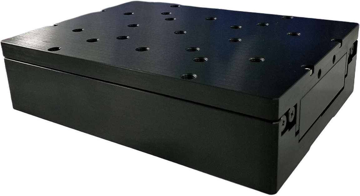
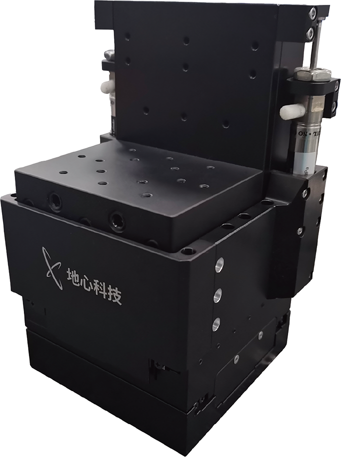
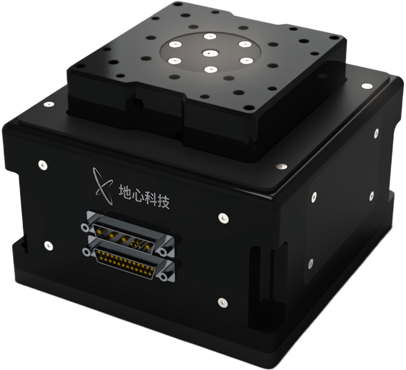
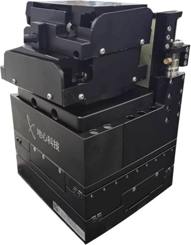
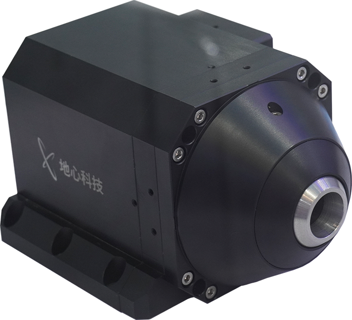
(1) 3‑Axis Fibre Scan Coupling
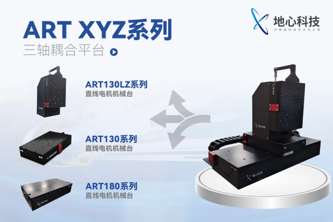
Product Features:
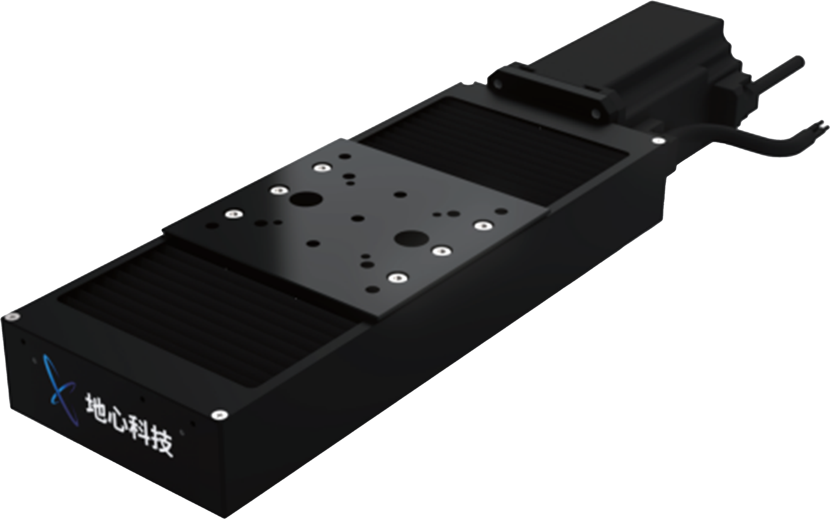
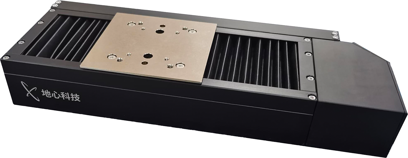
Self‑developed linear motor drive with fast response and high positioning accuracy
Compatible with high‑performance motion controllers to implement automatic light‑searching algorithms
High dynamic performance (cut‑off frequency >100 Hz)
Cross‑roller guides for high repeatability and fine stepping
Flexible travel configurations; XY integrated or discrete designs
Minimum step: 5 nm; repeatability: ±100 nm; positioning accuracy: ±250 nm
In‑position stability: 3 nm (configured with linear driver, in vibration‑isolated laboratory environment)
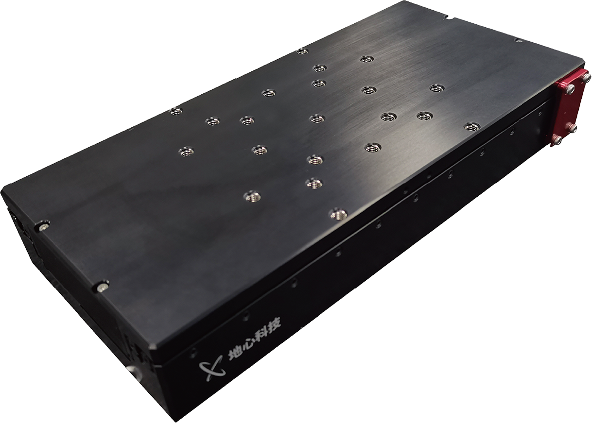
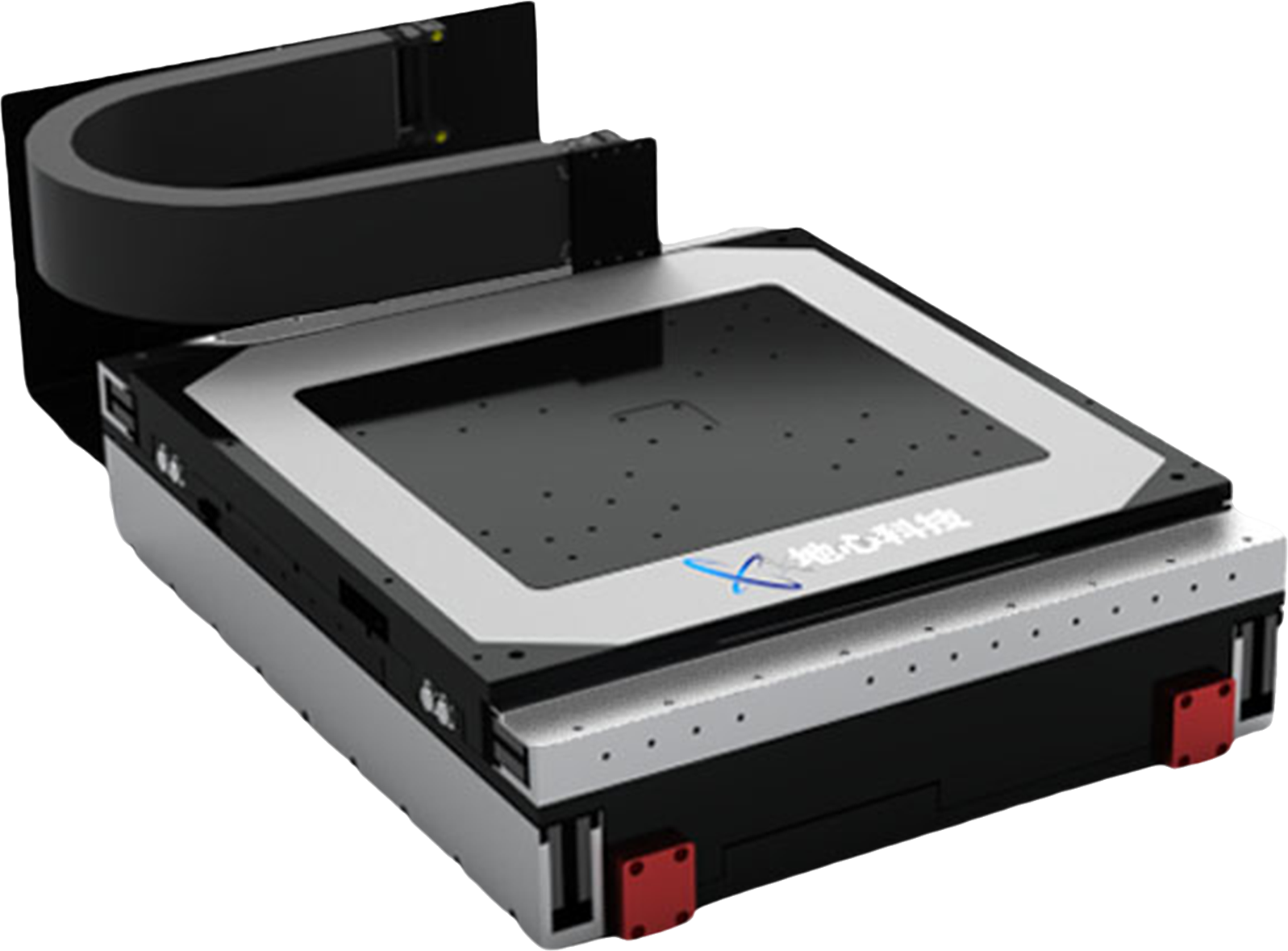
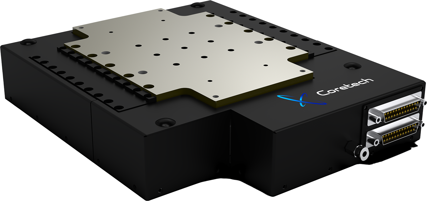
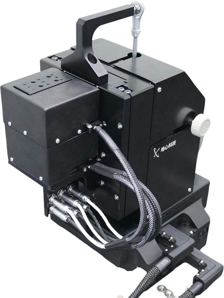
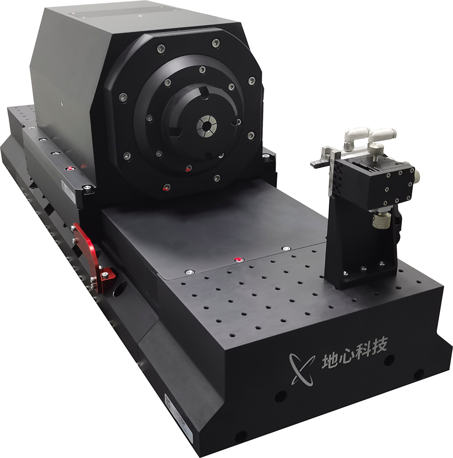
(2) 6‑Axis Fibre Scan Coupling
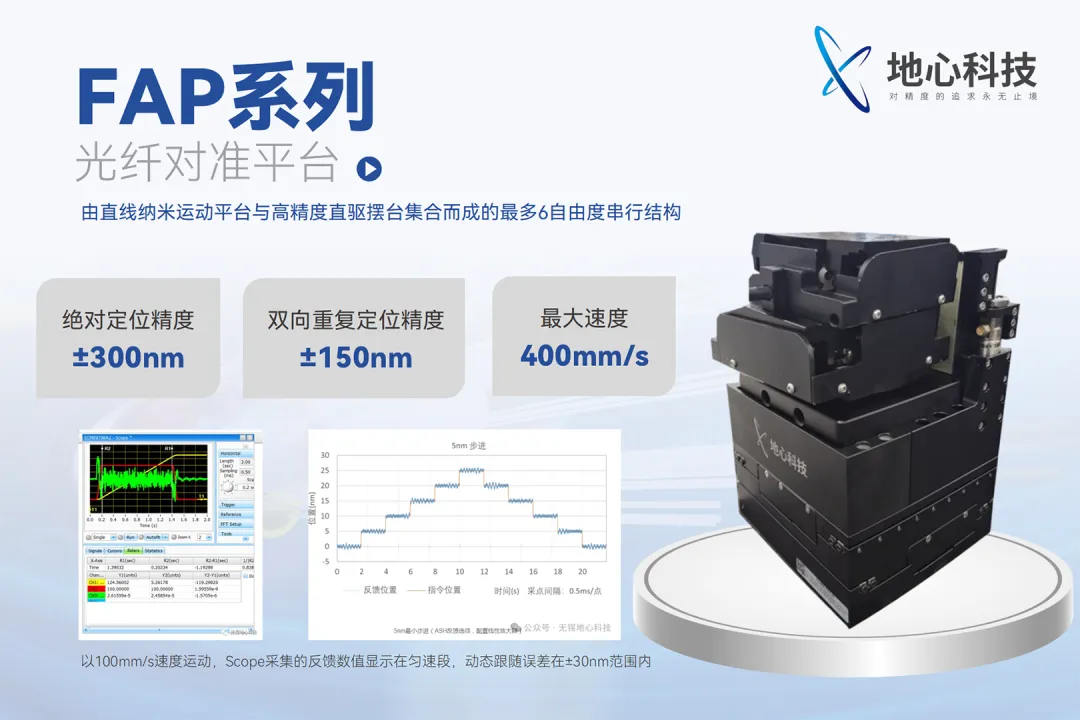
Product Features:
Based on integrated high‑performance ART series nano‑positioning stages
3 to 6 axes in series motion
All axes use non‑contact direct‑drive mechanisms to enhance throughput
Linear axis minimum step: 5 nm; rotary axis minimum step: 0.05 arc sec
Flexible configuration with multiple options
Equipped with analogue input interfaces for industry‑standard power meters
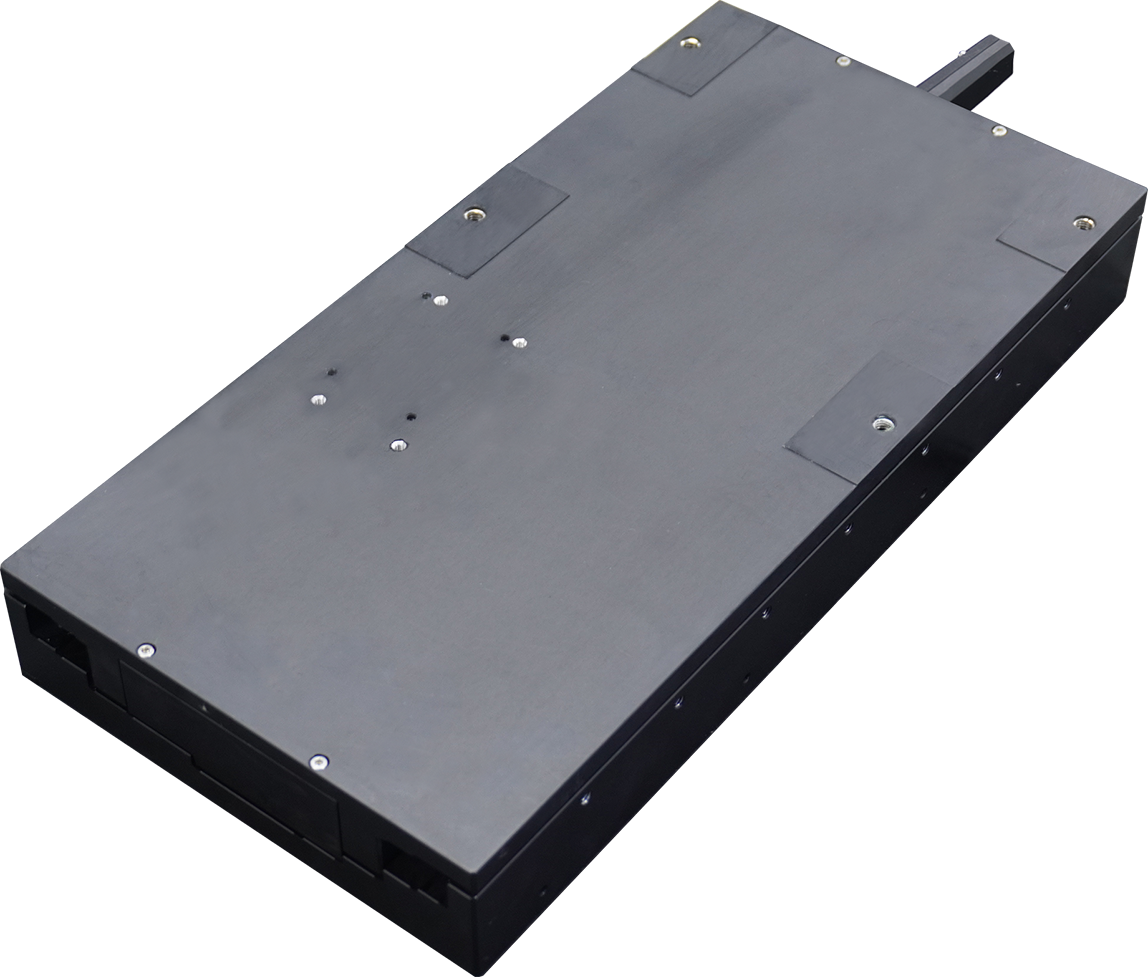
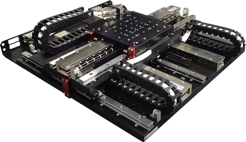
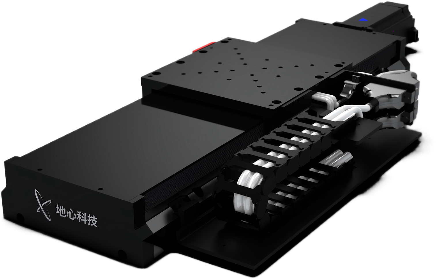
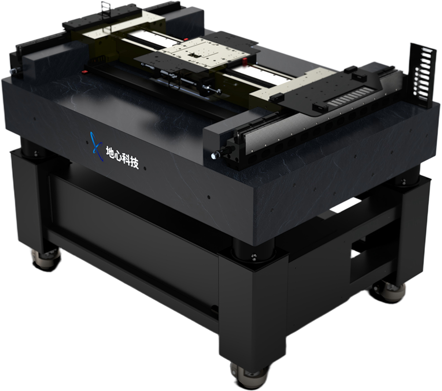
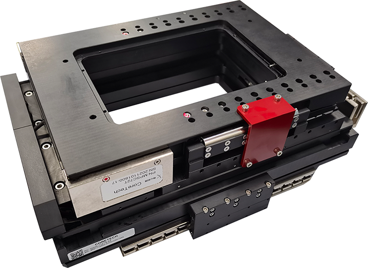
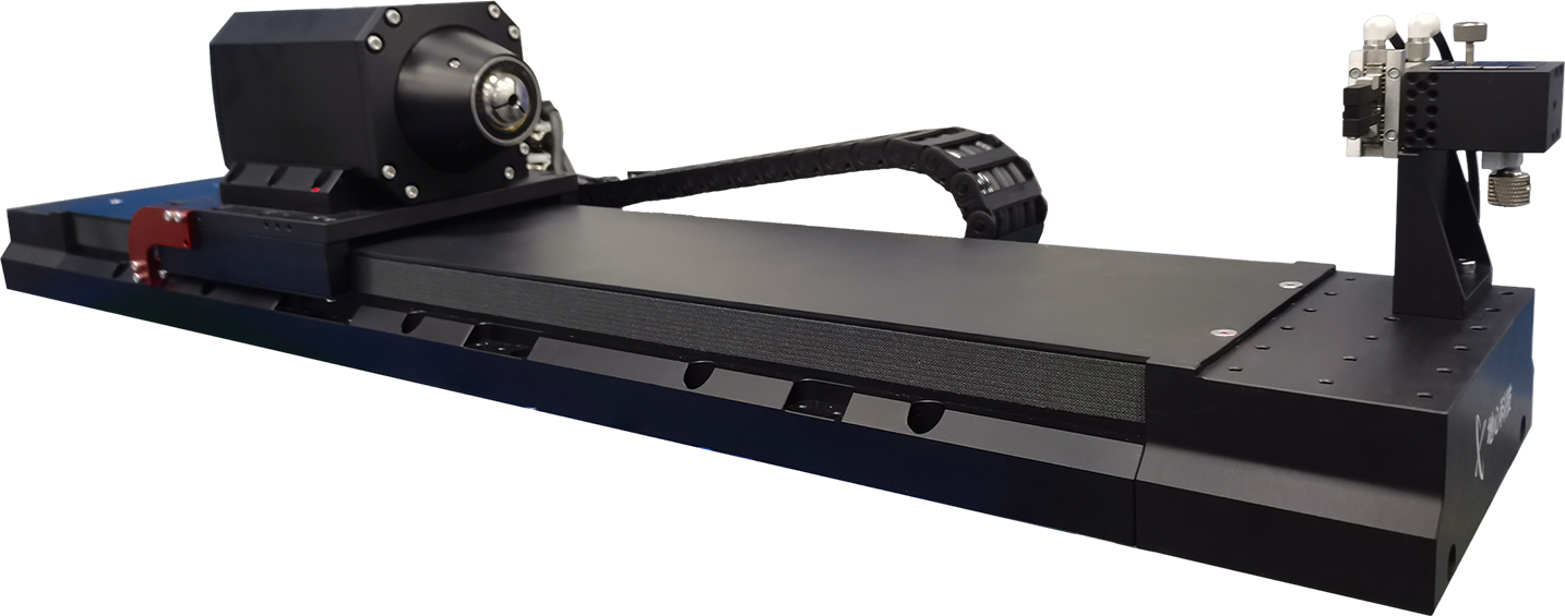
(3) Custom Wafer Bonding
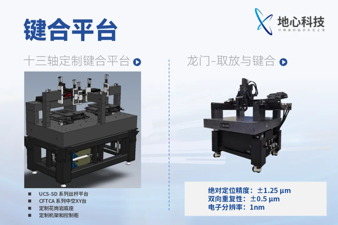
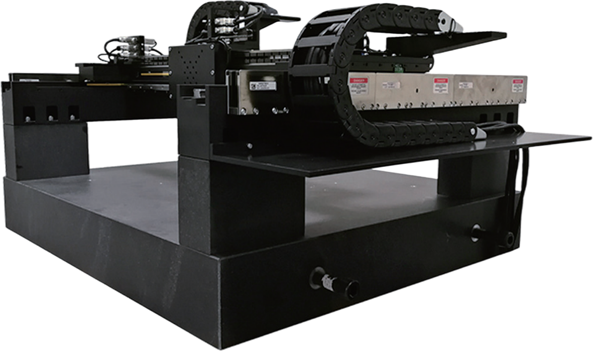
SLM1500 Series Gantry Product Features:
AC brushless dual‑drive motors
Travel ranges of dual‑drive axes and beam axis customisable to customer requirements
Maximum speed >2 m/s; maximum acceleration >2 g
Z‑axis and rotary axes with various travel and load options available per customer needs
Flexible cable management for optional cameras, air tubes, lasers, sensors, and other equipment
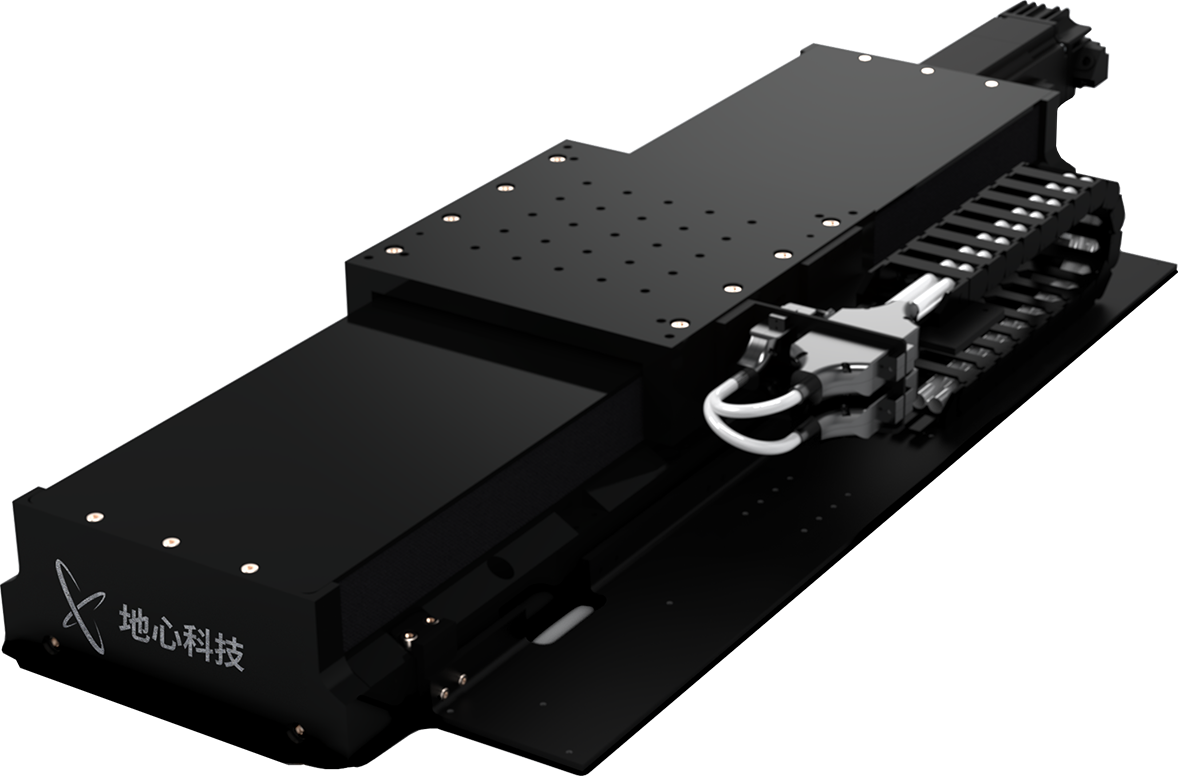
Dual‑drive axes optionally available as standard platforms or custom marble‑based solutions
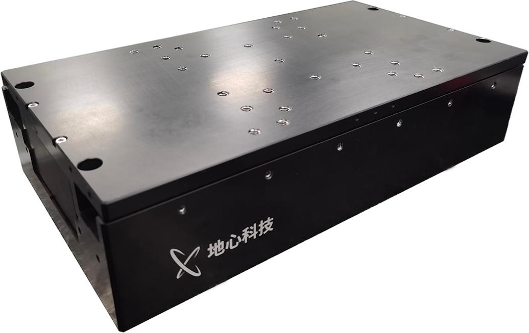
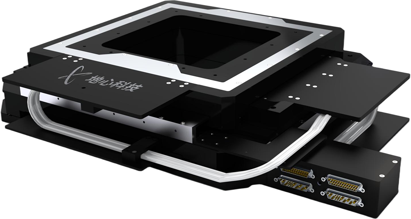
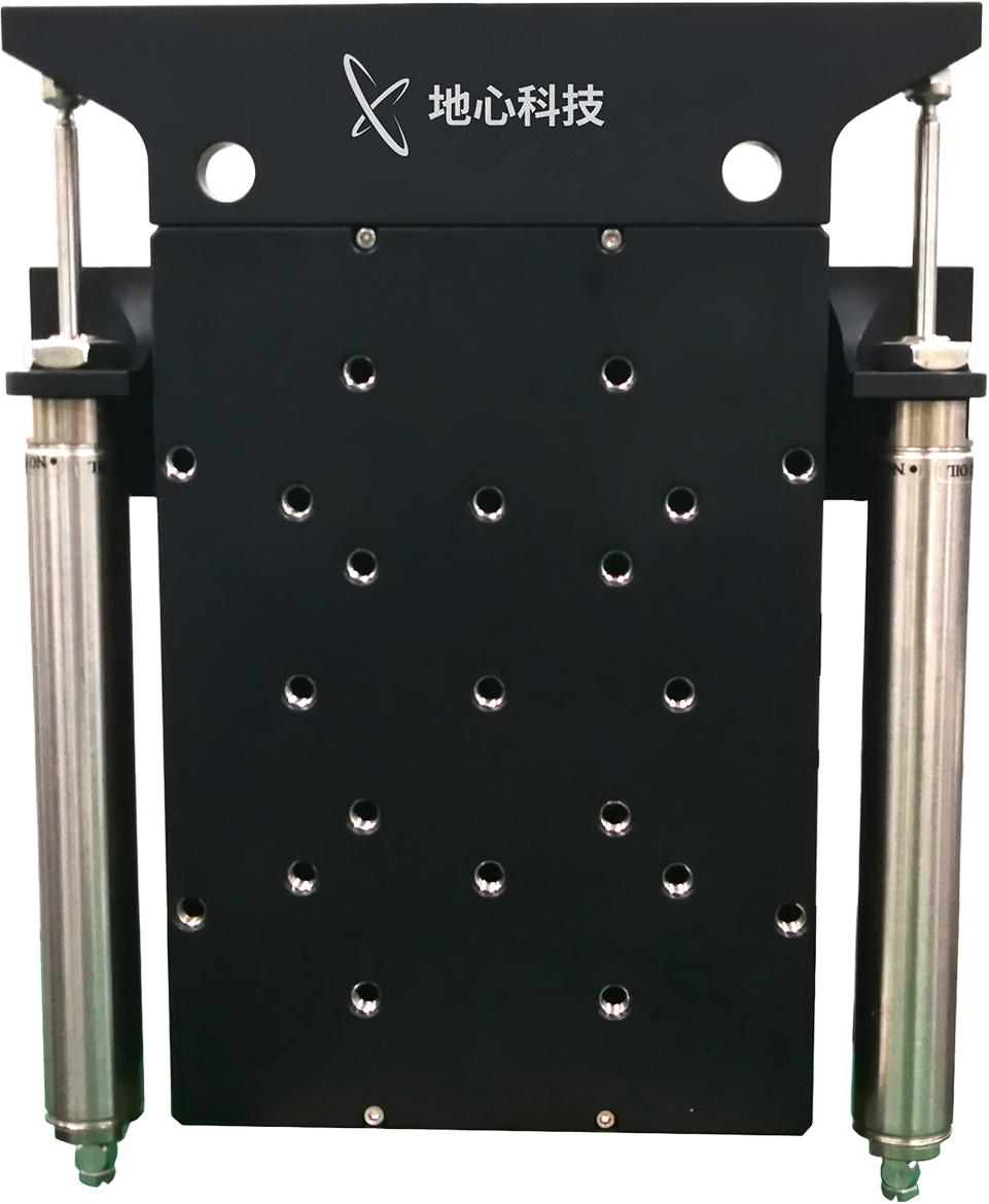
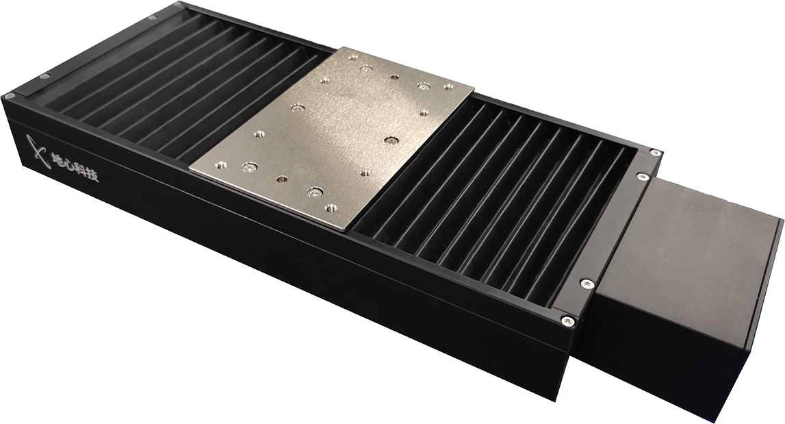
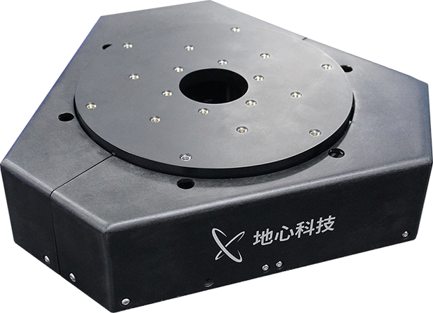
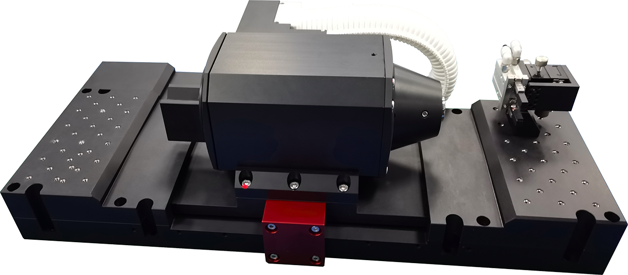
(4) Quantum Chip Laser Micromachining
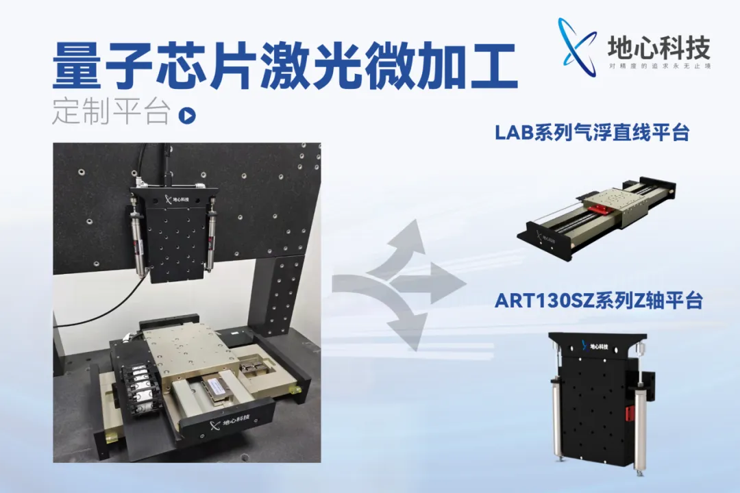
Product Features:
XY air‑bearing stage with stacked configuration
XY single‑axis straightness/flatness: ±0.5 μm
XY pitch/yaw/roll: <3 arcsec
XY repeatability: ±0.1 μm
Z‑axis with dual‑cylinder counterbalance, offering outstanding dynamic performance
Precision motion control platforms are not only core components of optical chip manufacturing equipment, but also key enablers driving optoelectronic technology toward higher integration and lower power consumption.
Whether it is the high‑speed optical modules in data centres that support AI computing power, or the co‑packaged optics (CPO) technology envisioned for future 6G networks, their manufacturing processes all depend on nanometre‑level precision motion control capabilities.
By providing reliable and efficient automated coupling solutions to optical module and chip manufacturers, Geocentric Technology is building a solid foundation for industry‑wide technological upgrades and cost control, helping China’s optical communications industry secure a more competitive position in the global market.
Featured News
Coretech Application | Large Aperture 2D Motion Stage Enhances Reticle Inspection Accuracy in Mask Lithography
2026.06.03
From Optical Chip Manufacturing to Fiber Coupling: Ultra‑Precision Motion Control Platforms Enabling a Technological Leap in the Optical Communications Industry
2026.06.03
Laser Processing Automation Solutions – 3D Spatial Drilling
2026.06.03
 Back to List