
.png)

.png)







Home
 News Center
Semiconductor Photomask Inspection: Beyond the Optical System, High-Precision Motion Stages Also Determine True Accuracy
News Center
Semiconductor Photomask Inspection: Beyond the Optical System, High-Precision Motion Stages Also Determine True Accuracy
News Center
Semiconductor Photomask Inspection: Beyond the Optical System, High-Precision Motion Stages Also Determine True Accuracy
Semiconductor Photomask Inspection: Beyond the Optical System, High-Precision Motion Stages Also Determine True Accuracy
 2026-06-02
Share:


The error of a single photomask can be replicated onto thousands of chips.
To clearly see, accurately measure, and determine whether a photomask is qualified, relying solely on a high-performance optical system is far from sufficient. In a sense, the upper limit of photomask inspection is determined not only by optical precision, but also jointly by the precision, stability, dynamic response, and cleanroom compatibility of the motion stage.
01 Advanced Process Demands Inspection First
As process nodes continue to shrink, pattern linewidths decrease, and stack structures grow increasingly complex, the photomask is no longer just a "pattern carrier"—it has become a core process object that directly impacts wafer yield, manufacturing cost, and product delivery capability.
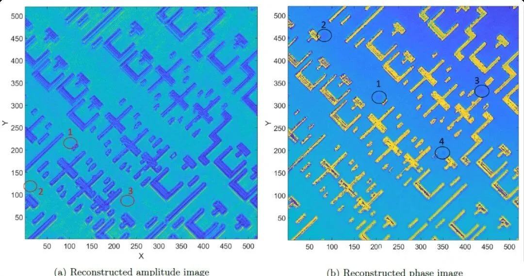
According to an industry report from a leading company, as chip processes continue to scale down, the number of photomasks required for advanced 14nm/10nm nodes can reach 60 layers, while 28nm requires 50 layers, and 130nm requires 30 layers. The increase in layer count means that process complexity, data volume, inspection and repair difficulty, and delivery requirements all escalate correspondingly.
According to data from Guosheng Securities, the current localization rate for semiconductor photomasks in China is approximately 10%, and for mid-to-high-end photomasks, it is only 3%. The market is dominated by overseas manufacturers such as Photronics (USA), DNP (Japan), and Toppan (Japan).
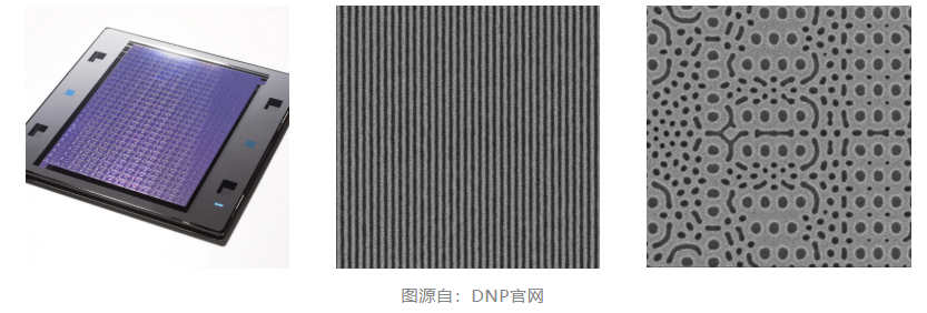
Leading global photomask manufacturers and inspection equipment companies are continuously increasing investments in advanced mask and defect inspection capabilities. Photomasks are evolving from a "critical material" to a "core yield-control link."
02 Throughout the Process: Why the Motion Stage Matters
In the lithography process, the pattern on the photomask is transferred to the wafer through the exposure system, and then through etching, deposition, ion implantation, and other steps, the chip structure is gradually formed. In other words, any pattern defect, dimensional error, positional deviation, particle contamination, or phase issue on the photomask may be repeatedly replicated onto a large number of chips.
Unlike ordinary industrial plates, semiconductor photomasks have smaller feature sizes, more layers, and exceptionally high requirements for CD (Critical Dimension) uniformity, overlay accuracy, defect control, and cleanliness. A high-end photomask is often extremely valuable, and once a defective mask is used on the production line, the loss is far greater than just the cost of "remaking a mask"—it can result in yield drops across entire wafer batches, delivery delays, and even supply chain risks.
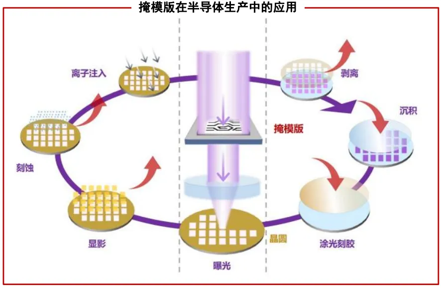
Therefore, photomask inspection is not an "optional" step, but a necessary quality gateway in both mask manufacturing and usage. Photomask inspection is essentially a collaborative engineering effort between "optical/imaging systems" and "precision motion systems." The motion stage is not merely a material handling component; it is the core execution unit within the inspection chain.
From pre-alignment and reference establishment, to full‑field scanning, fine re‑inspection, autofocus, defect revisiting, CD measurement, and post‑repair re‑testing, photomask inspection is responsible not only for "moving the mask into position," but also for critical tasks such as coordinate establishment, stable scanning, field stitching, focal plane maintenance, defect repositioning, and multi‑module coordination.
| Inspection Step | Role of the Motion Stage | Accuracy Requirement |
|---|---|---|
| Fine Alignment / Reference Setup | Establish coordinate system and reference mark recognition | Sub‑micron to hundreds of nanometers |
| Full‑Field Scanning | Large‑stroke stable scanning | Dynamic sub‑micron tracking capability |
| Zone Fine Scanning | High‑magnification, high‑resolution scanning of critical areas, suspect regions, and key pattern zones | Sub‑micron positioning / repeatability |
| Image Stitching | Precisely control displacement between adjacent fields; reduce transfer of rotation errors, scaling errors, and geometric distortion | Sub‑micron step accuracy |
| Autofocus / Z Compensation | Real‑time focal plane adjustment to maintain clear imaging | Sub‑micron Z‑axis resolution / repeatability |
| Defect Re‑Inspection | Ensure re‑inspection field accurately covers defect locations, improving review efficiency and consistency | Sub‑micron to within a few microns |
| CD Measurement | Support edge extraction, linewidth measurement, contour analysis; work with focusing system to acquire high‑quality images | High sub‑micron or even higher |
| Overlay‑Related Measurement | Precisely move to multiple measurement points to support high‑consistency sampling across regions | Sub‑micron |
| Pre‑Repair Positioning | Feed defect coordinates into the repair field of view | High repeatability positioning |
| Post‑Repair Re‑Test | Return to original location for re‑evaluation | Sub‑micron |
| Post‑Clean Re‑Inspection | Detect at the same point again | High repeatability positioning |
| Calibration / Standardization | Establish error compensation models | High repeatability and stability |
03 Large‑Aperture Motion Stages: A Precise Breakthrough
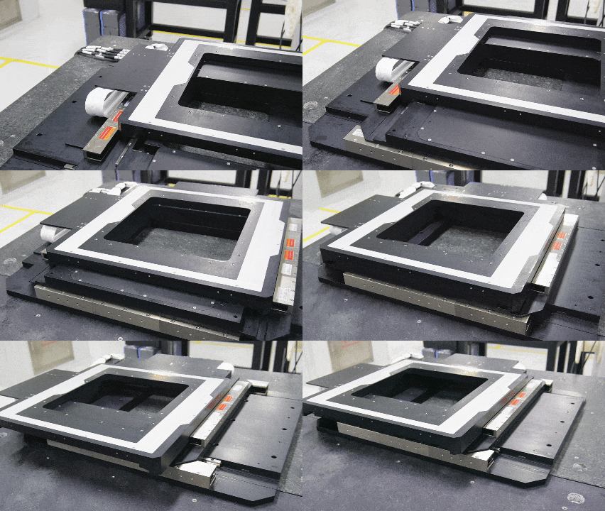
In this competition centered on precision, stability, and system synergy, the precision motion stage is no longer a supporting component—it has become the critical infrastructure that defines equipment performance boundaries.
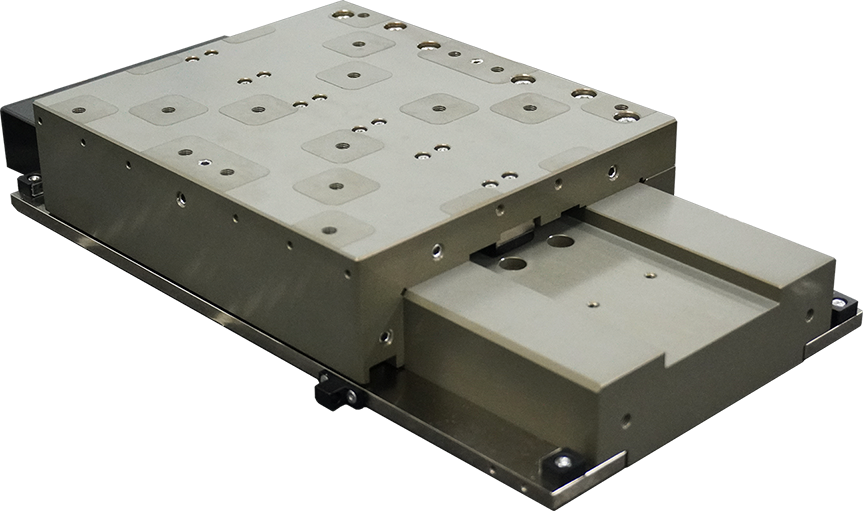
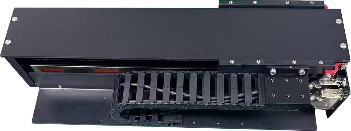
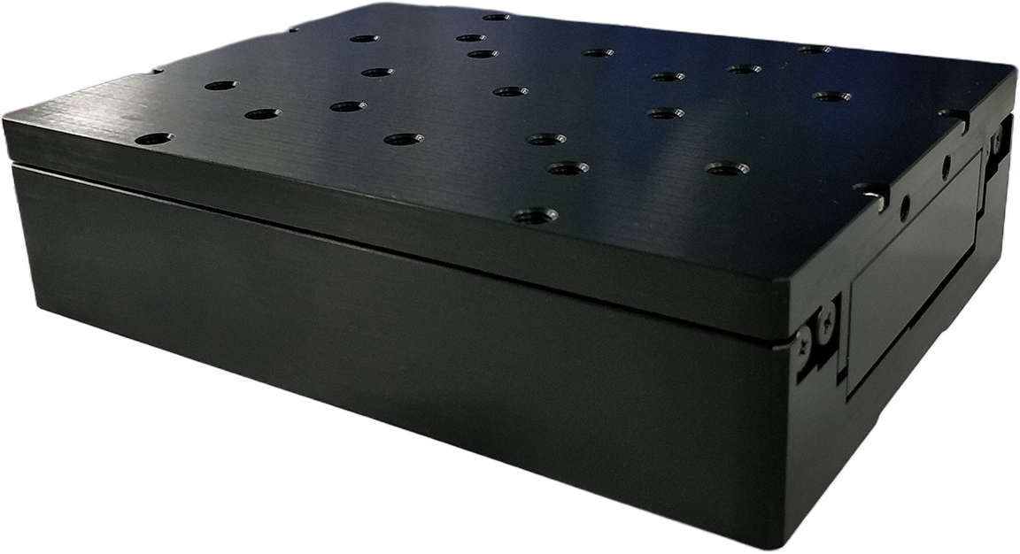
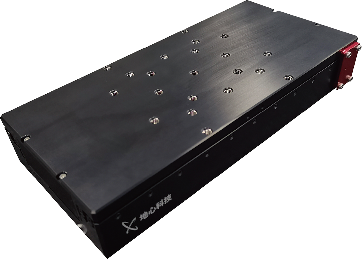
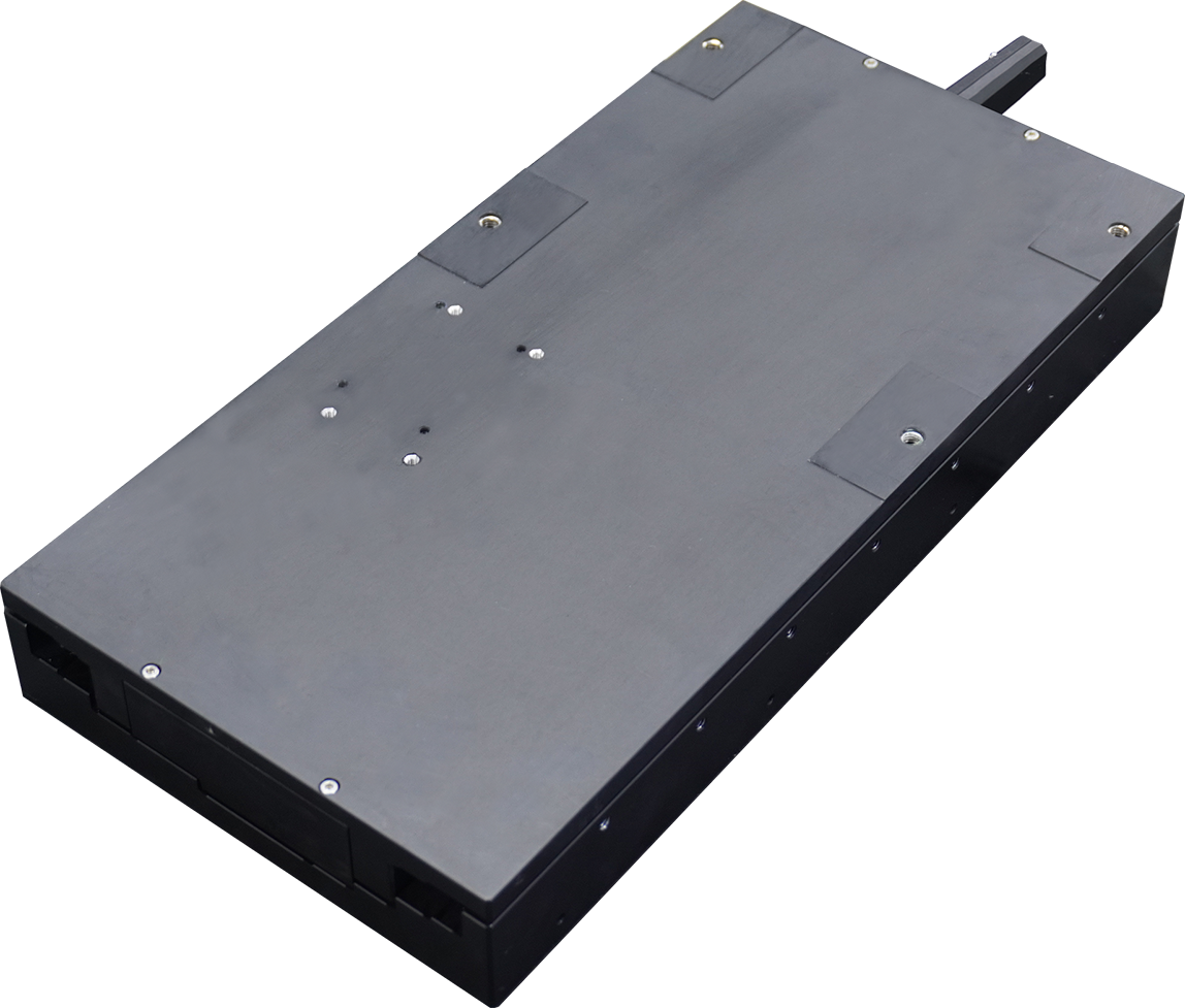
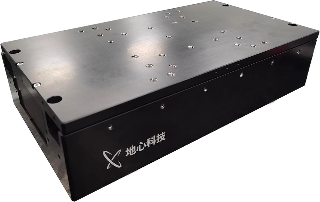
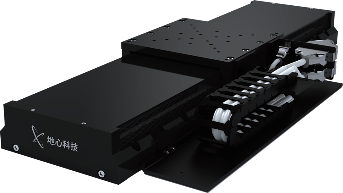
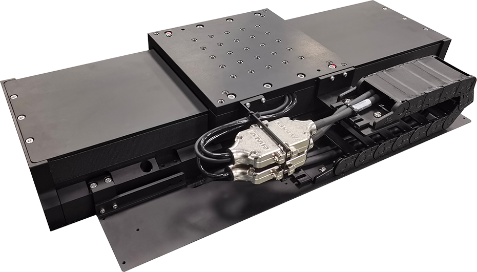
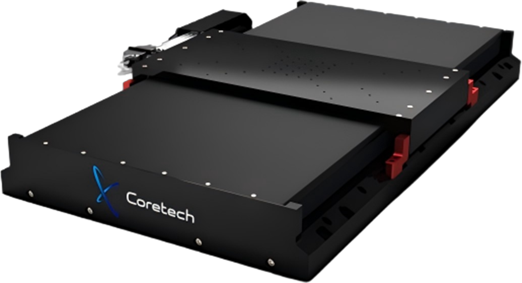
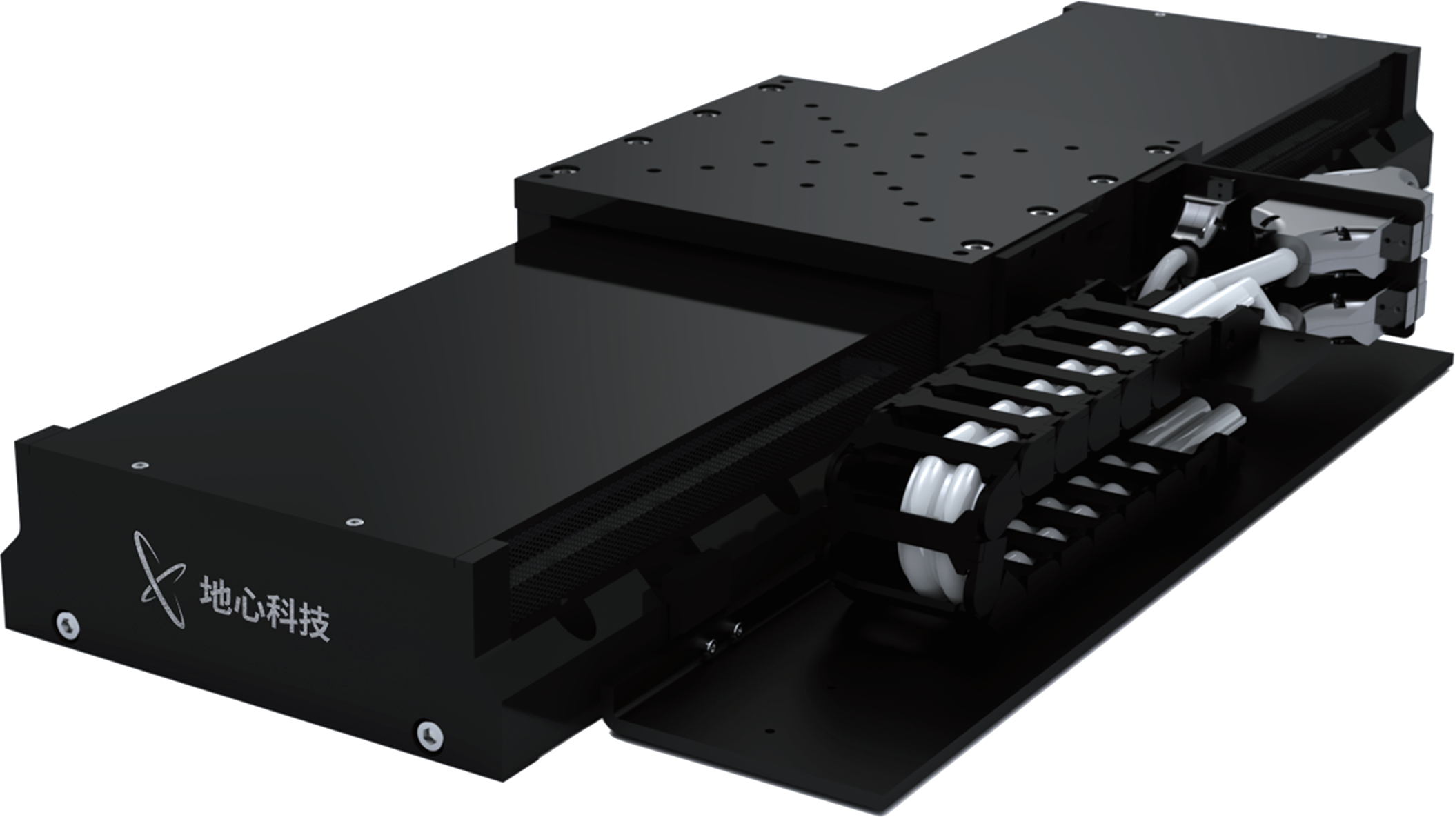
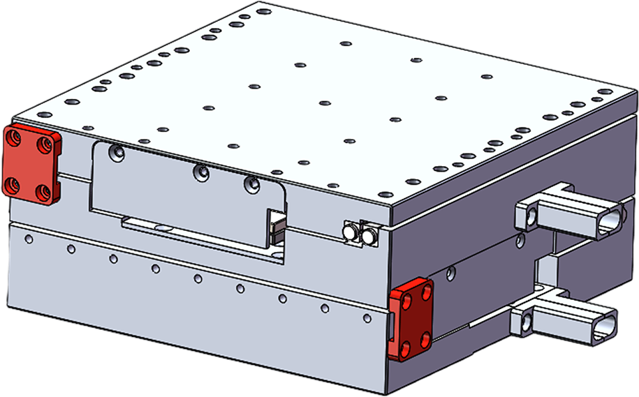
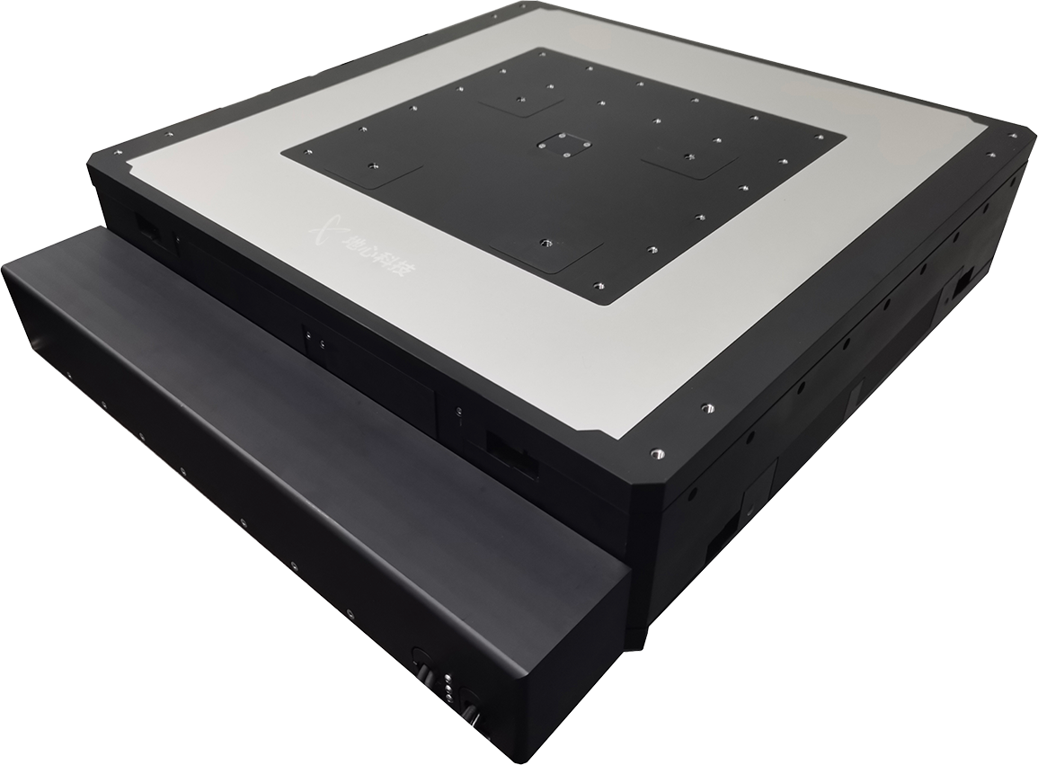
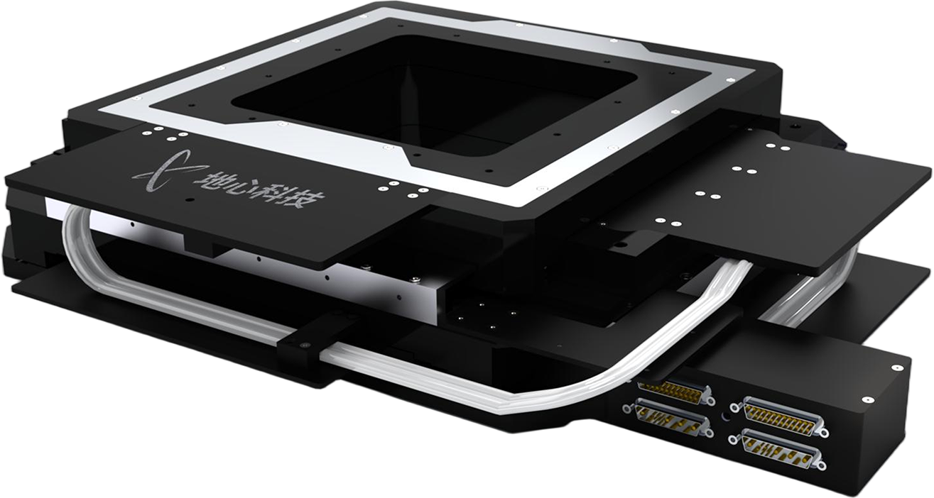
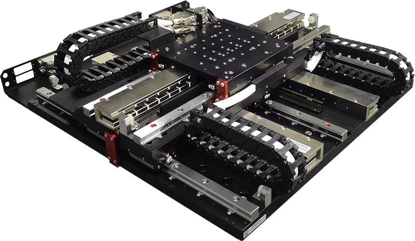
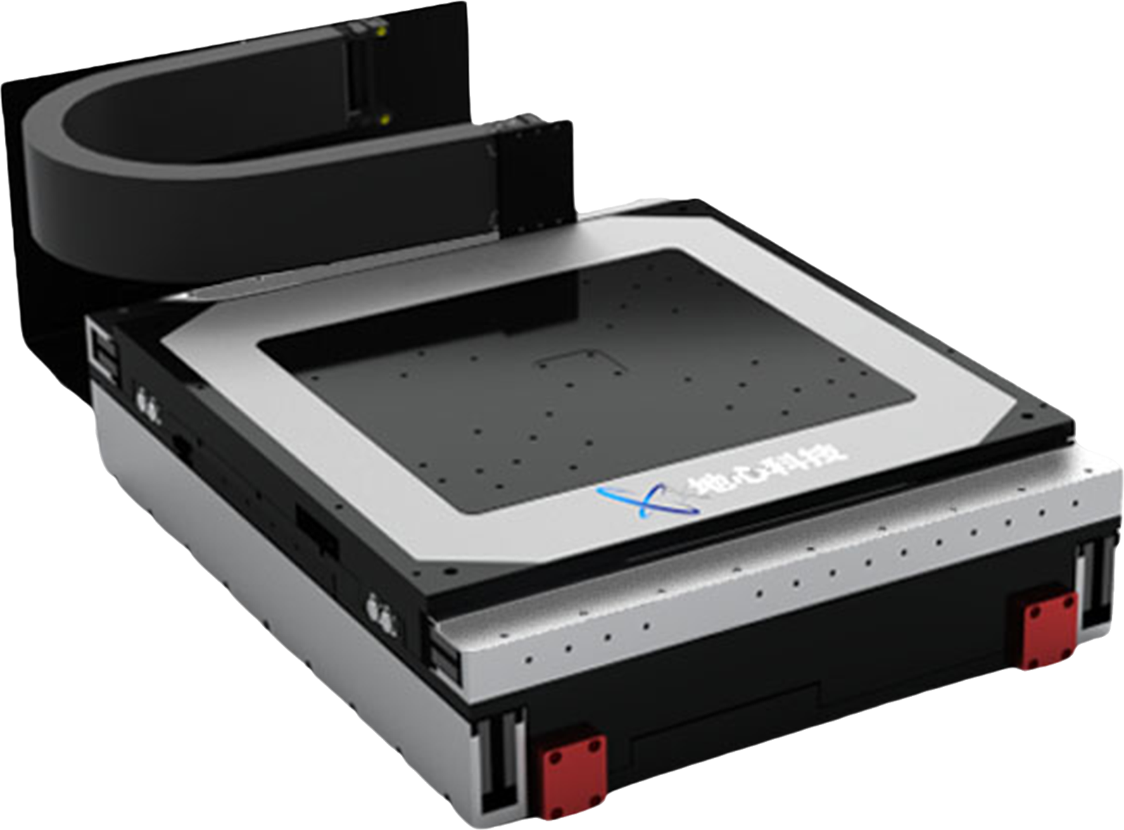
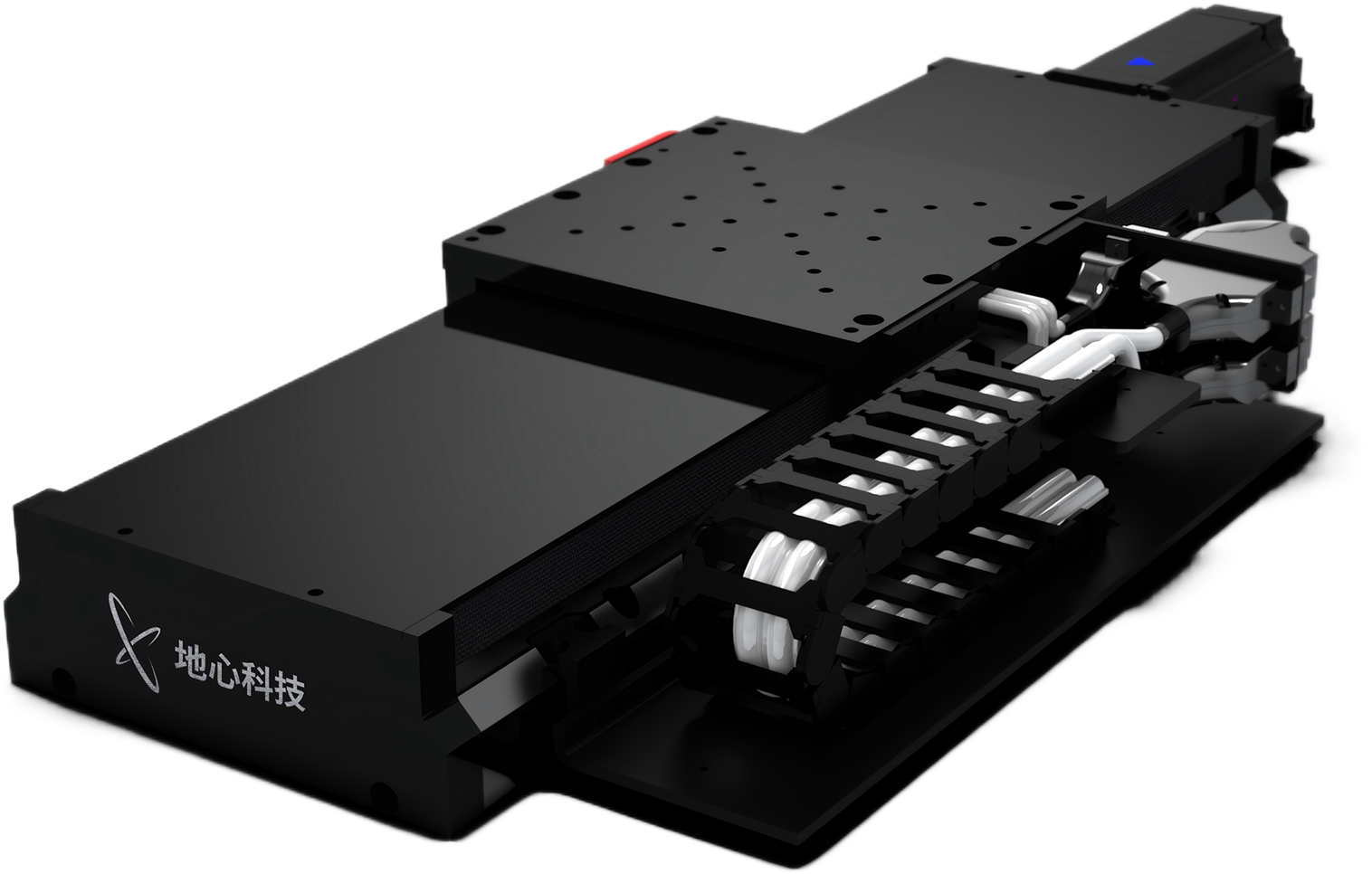
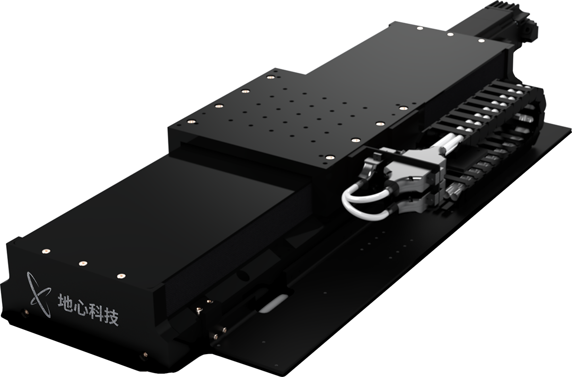
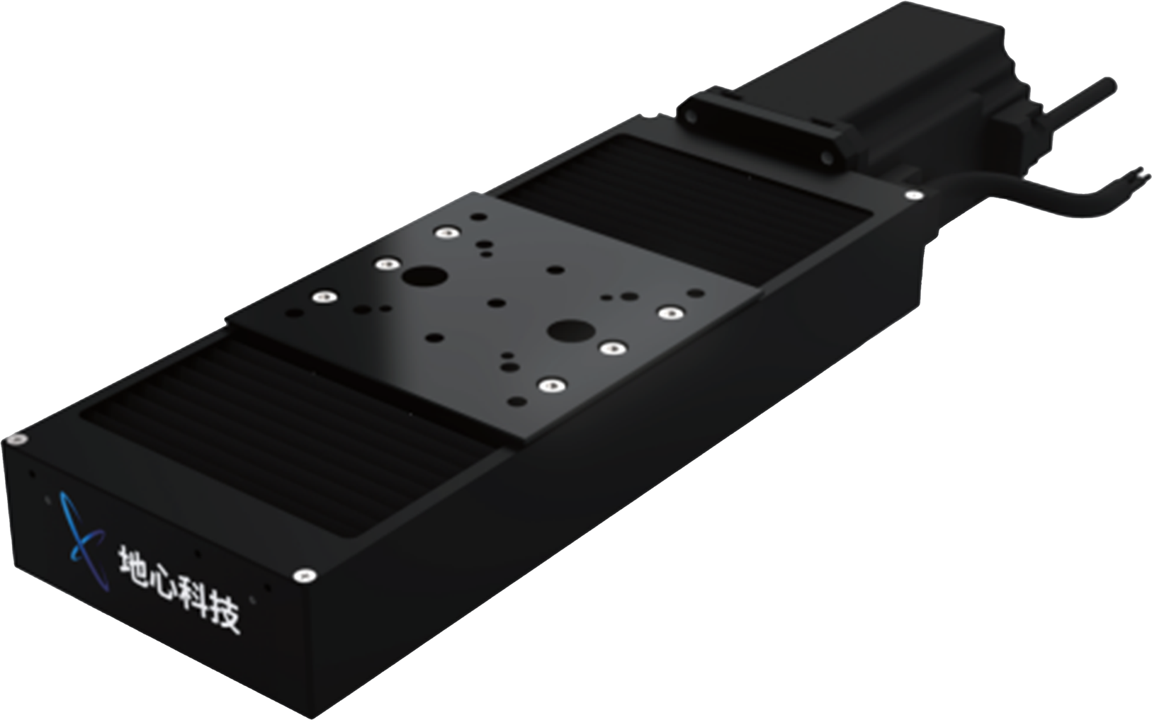
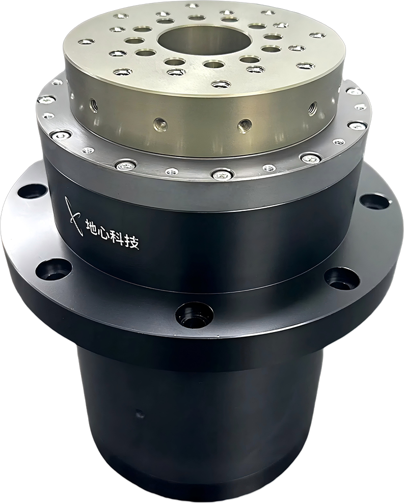
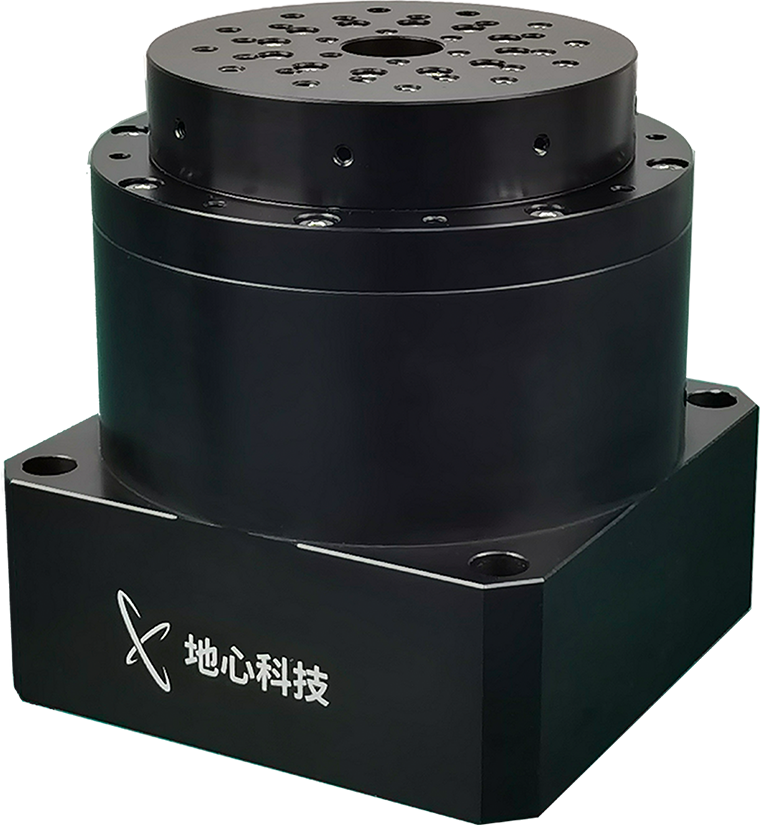
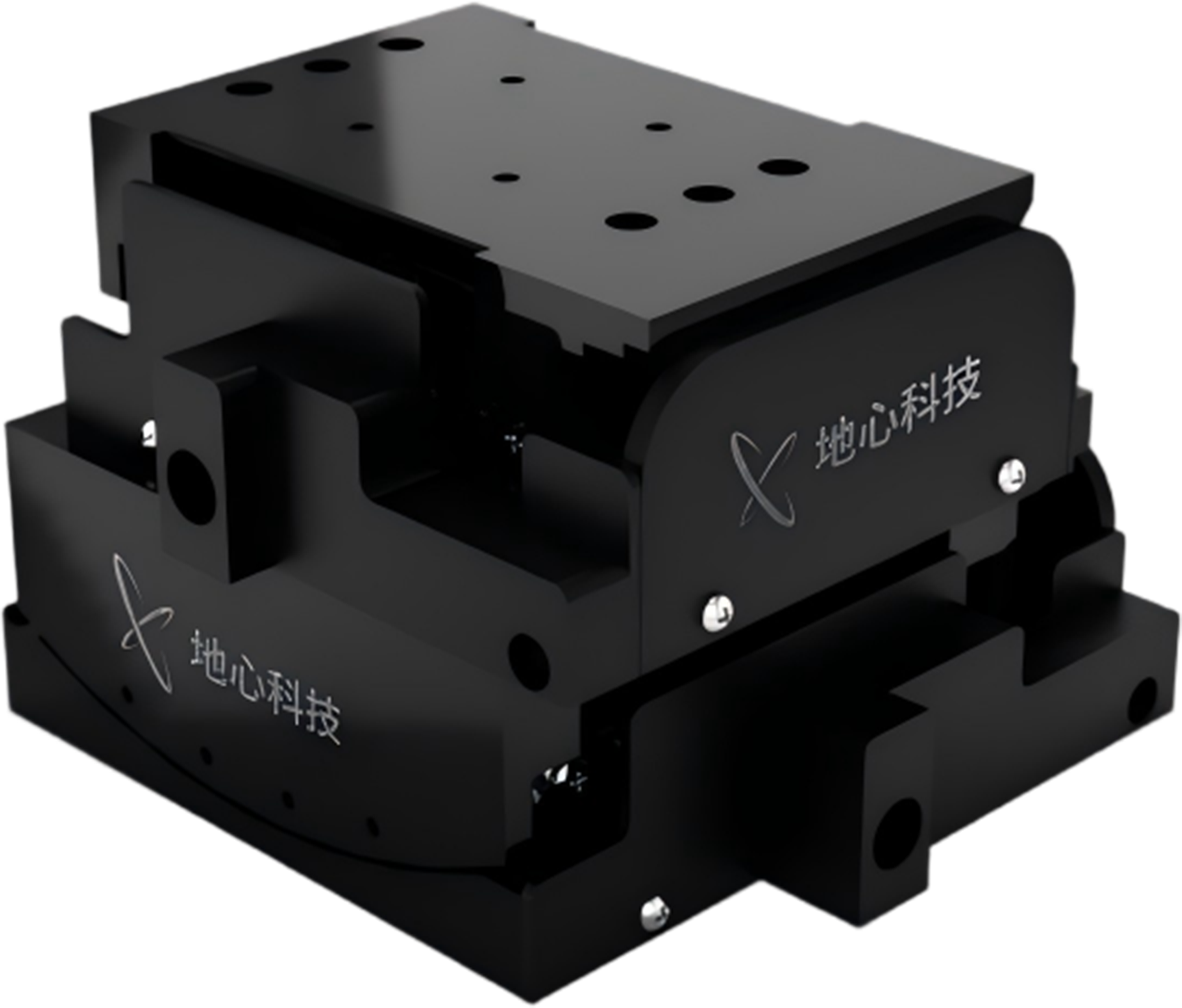
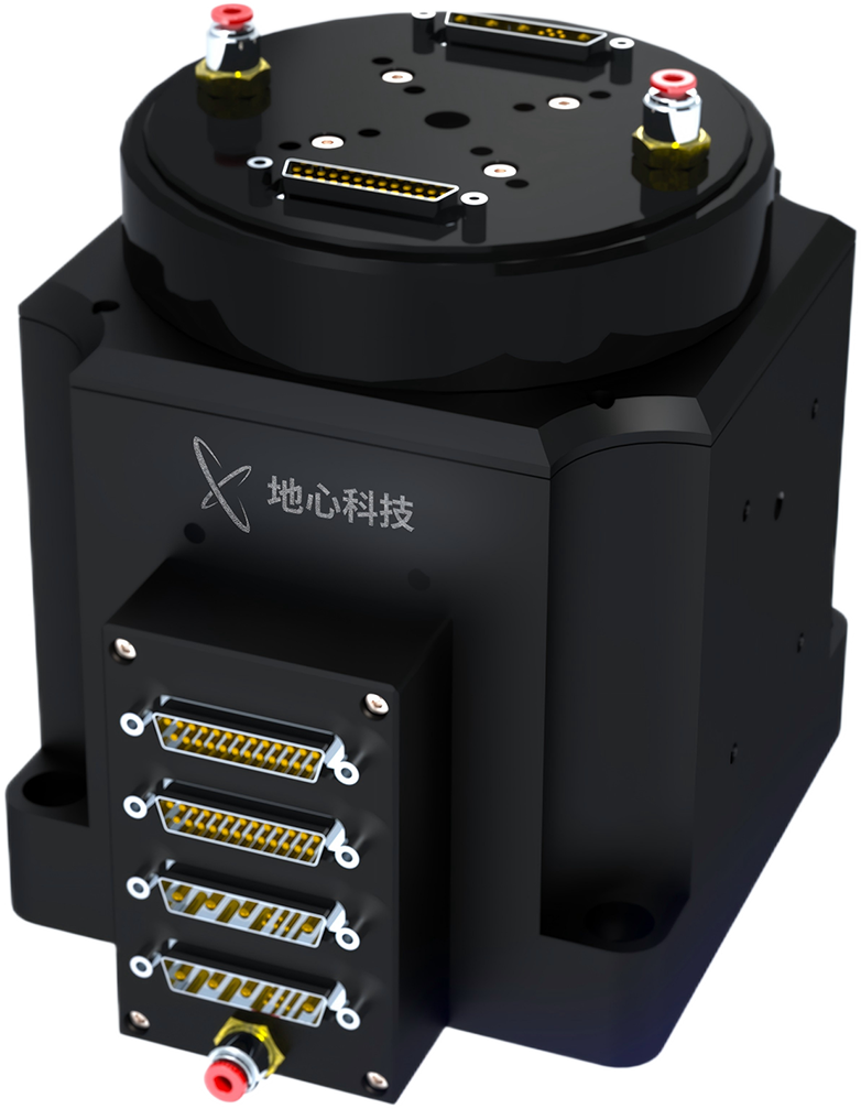
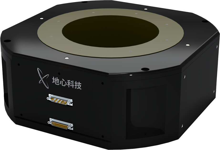
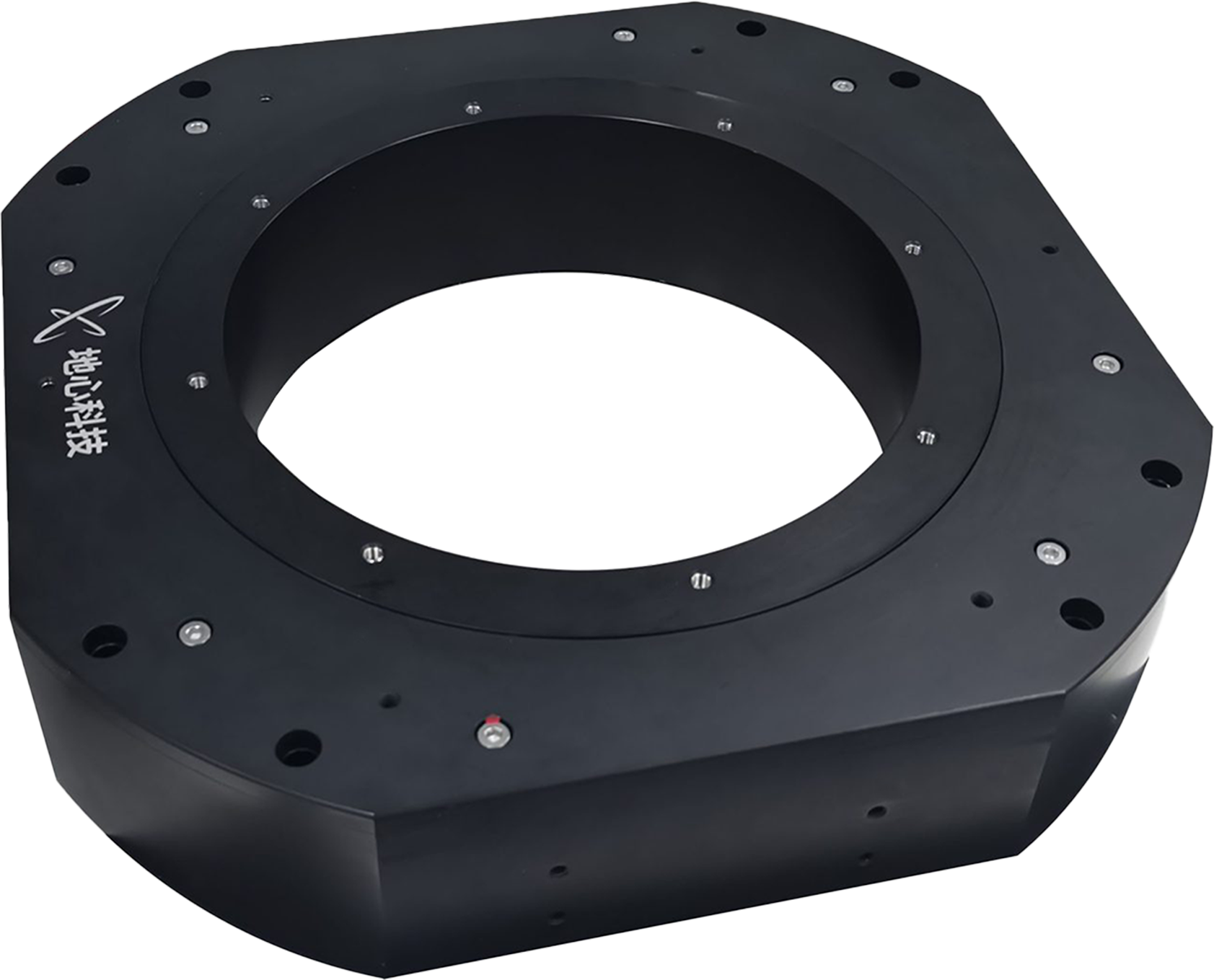
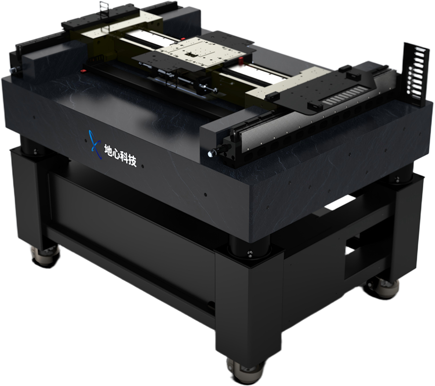
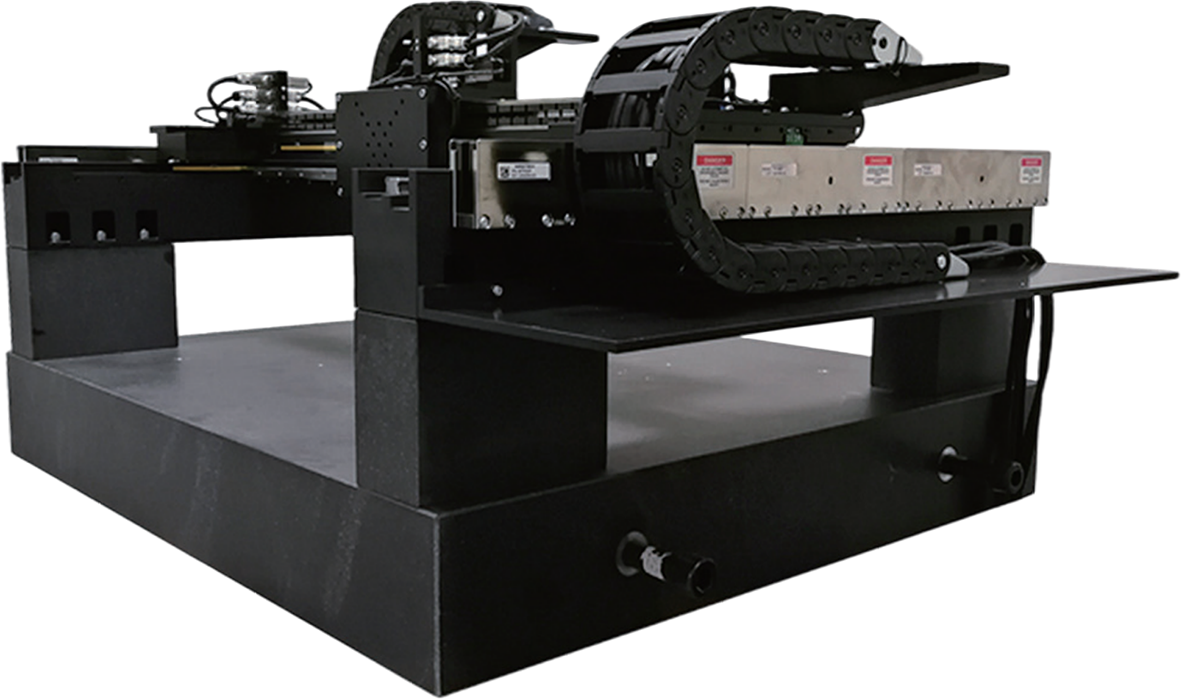
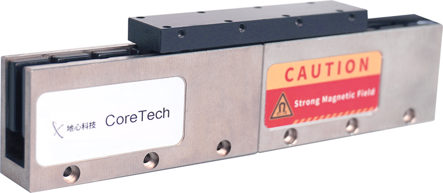
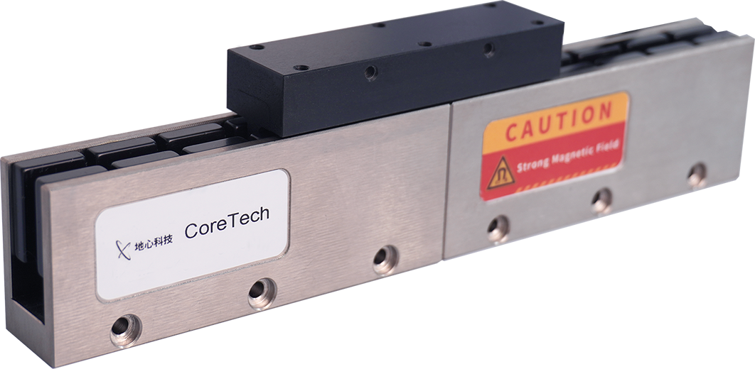
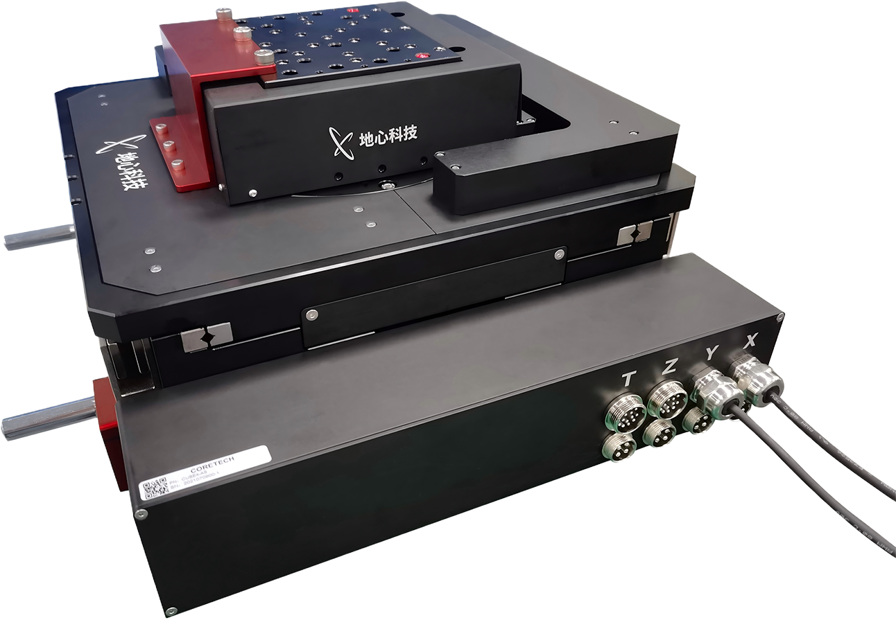
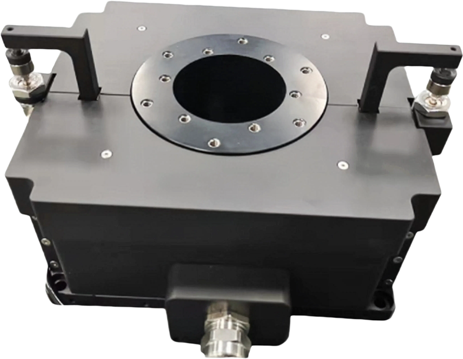
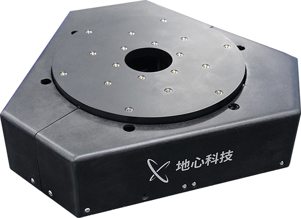
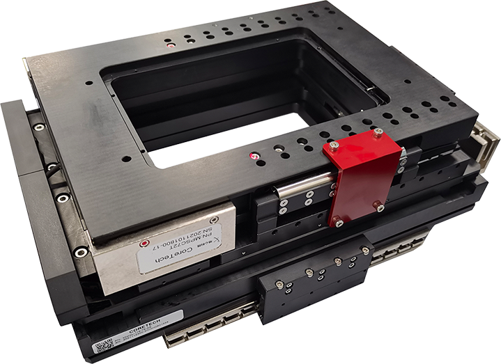
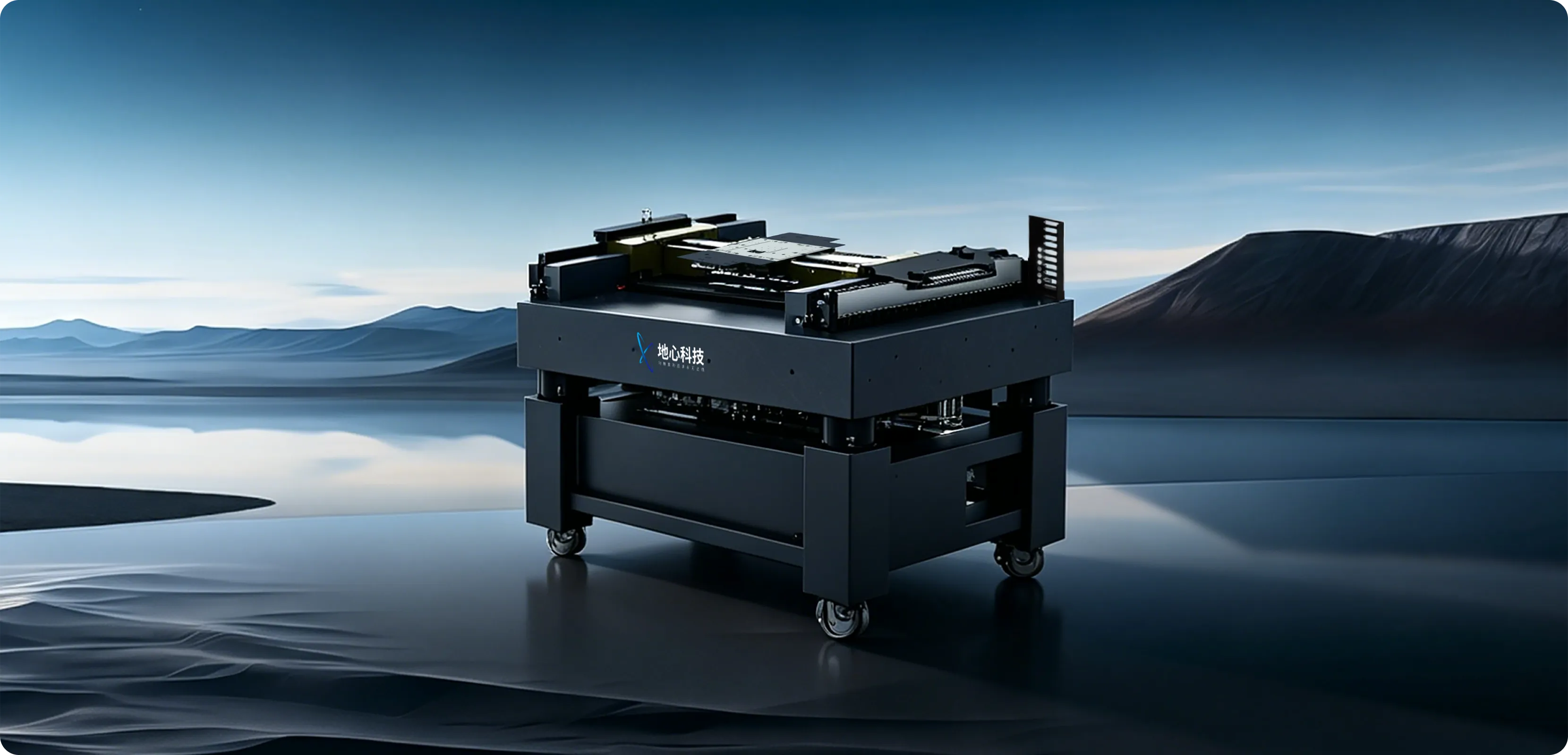
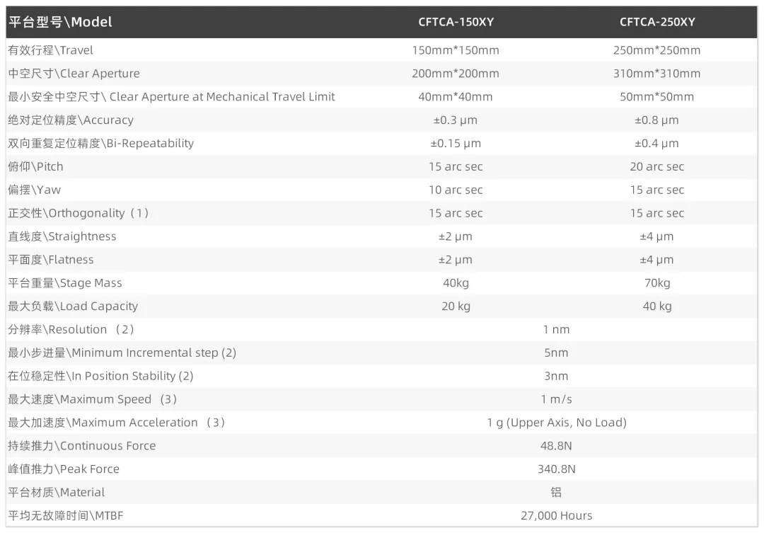
With years of deep engagement in the semiconductor industry, Ground Motion Technology offers the CFTCA series large‑aperture XY motion stages, precisely tailored for photomask inspection applications that demand stringent optical path requirements. As a large‑aperture, integrated XY precision positioning stage with nanometer‑level accuracy, the CFTCA series employs linear motor drives and precision crossed‑roller bearings, delivering excellent dynamic performance and positioning accuracy, with an unloaded cutoff frequency exceeding 100 Hz.
The stage combines compact construction with robust driving capability: the upper axis achieves a maximum speed of 1000 mm/s and an unloaded acceleration of up to 1g. When configured with linear amplifiers and operating in a vibration‑isolated laboratory environment, the CFTCA series achieves in‑position stability of 3 nm and a minimum step size of less than 5 nm.
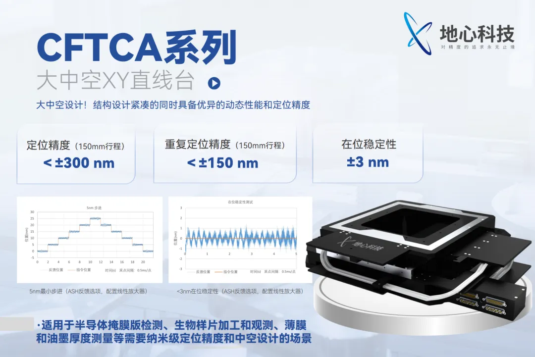
The large clear aperture of the stage provides generous open space, offering greater flexibility for optical paths, cameras, sensors, air lines, vacuum channels, or auxiliary inspection modules.
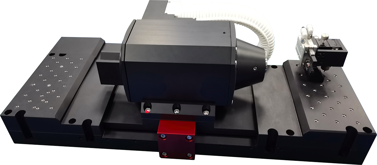
Therefore, it is particularly well‑suited for semiconductor photomask inspection equipment that demands high system layout flexibility, inspection efficiency, and stability. In photomask inspection systems, Ground Motion Technology's large‑aperture stage serves as a highly stable, precise, and compatible motion base for the optical inspection system, enabling complex optical paths, upper‑lower module coordination, and precision scanning to be efficiently realized on a single platform architecture.
Featured News
From Optical Chip Manufacturing to Fiber Coupling: Ultra‑Precision Motion Control Platforms Enabling a Technological Leap in the Optical Communications Industry
2026.06.03
One Article Summary | Multiple Applications of Precision Motion Stages in Wafer Defect Inspection
2026.06.03
Laser Processing Automation Solutions – Laser Micro/Nano Machining
2026.06.03
 Back to List