
.png)

.png)







Home
 News Center
Wafer Defect Inspection: Solving the "Auto‑Focus Tracking" Challenge to Improve Detection Accuracy and Efficiency
News Center
Wafer Defect Inspection: Solving the "Auto‑Focus Tracking" Challenge to Improve Detection Accuracy and Efficiency
News Center
Wafer Defect Inspection: Solving the "Auto‑Focus Tracking" Challenge to Improve Detection Accuracy and Efficiency
Wafer Defect Inspection: Solving the "Auto‑Focus Tracking" Challenge to Improve Detection Accuracy and Efficiency
 2026-06-03
Share:


"Coretech's high‑precision ONEXY series XY integrated linear motion stage, paired with the SurfaceZ series high‑precision Z‑lift stage, perfectly addresses the challenge of rapid auto‑focus tracking in wafer defect inspection applications, and enables equally spaced triggering of high‑speed cameras for image acquisition, playing a vital role in the field of wafer defect inspection."
01 AOI Wafer Defect Inspection
Wafer defect optical inspection has long been an engineering challenge that evolves alongside IC manufacturing development. Wafer defect inspection must accurately identify defects such as voids, pits, and scratches, and obtain detailed information including defect location, area size, and more. It must also meet the speed and throughput requirements of large‑scale industrial production to achieve rapid inspection.
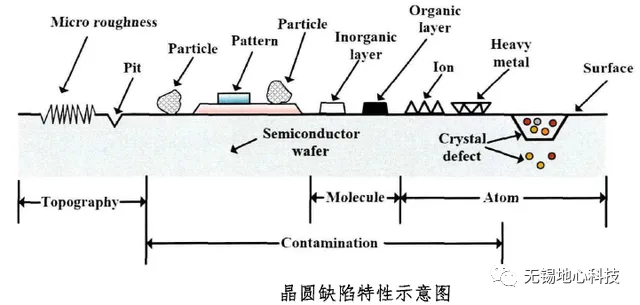
Image source: "Research on Multi‑Scan Patterned Wafer Inspection Technology Based on Bright‑Field and Dark‑Field Imaging" by Chen Shiwei (removed upon request)
In our previous application introductions, we discussed two common methods for wafer defect inspection in the semiconductor industry: Automated Optical Inspection (AOI) and Scanning Electron Microscope (SEM) systems. Today, we focus on a key challenge in AOI systems: auto‑focus tracking.
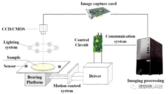
Schematic diagram of a typical AOI inspection system
02 Depth of Field in AOI Inspection Systems
In AOI inspection systems, imaging quality is critical for defect recognition. Current chip production processes typically require wafer defect inspection equipment to achieve measurement speeds exceeding 100 wafers per hour. At the same time, as semiconductor processes continue to improve, inspection systems are required to resolve defects down to 1 μm or even 0.5 μm.
For an imaging system, maximum resolution is achieved only at the focal plane. Therefore, the wafer under inspection should ideally remain at the focal plane at all times. However, due to microscopic surface topography variations, the wafer is never perfectly flat. In addition, factors such as vibration and structural thermal effects during system operation make it difficult to maintain perfect focus. As a result, the imaging system must possess a certain depth of field (DOF).
The depth of field of a lens is its ability to maintain the required image quality (spatial frequency at a specified contrast) as the object moves closer to or farther from the best‑focus position without requiring refocusing. In general, higher imaging system resolution results in shallower DOF. The DOF of AOI systems for wafer inspection is typically within 10 μm, meaning the relative positional deviation between the wafer and the lens must be kept within 10 μm.
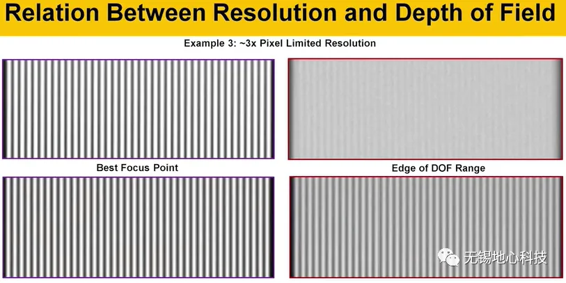
Relationship between DOF and resolution (Image source: Edmund Optics, removed upon request)
03 The Effect of Wafer Warpage
Wafers are subjected to mechanical stress during various process steps. In most cases, unbalanced stress on the front and back surfaces leads to warpage. This is particularly evident in grinding processes, where strong residual stresses can cause convex warpage (positive warp) or concave warpage (negative warp). Additionally, due to processing tolerances, wafer thickness can vary within a certain range.
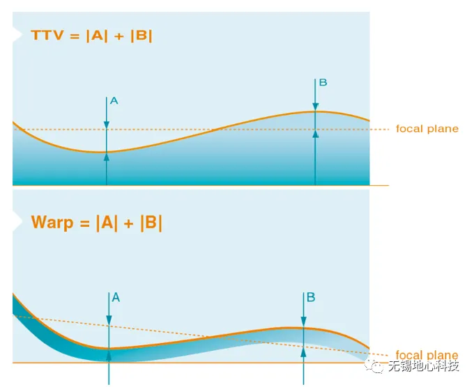
Wafer thickness variation and warpage
In conventional inspection systems, for wafers with warpage exceeding a certain level, focus is typically set at the wafer edge. This is done so that whenever the wafer moves into the camera's field of view, the camera can be triggered for sampling immediately, improving inspection efficiency. However, the consequent issue is that due to warpage, while the wafer edge remains within DOF, a large portion of the wafer centre falls outside DOF. This results in poor imaging quality due to defocus, leading to missed defects.
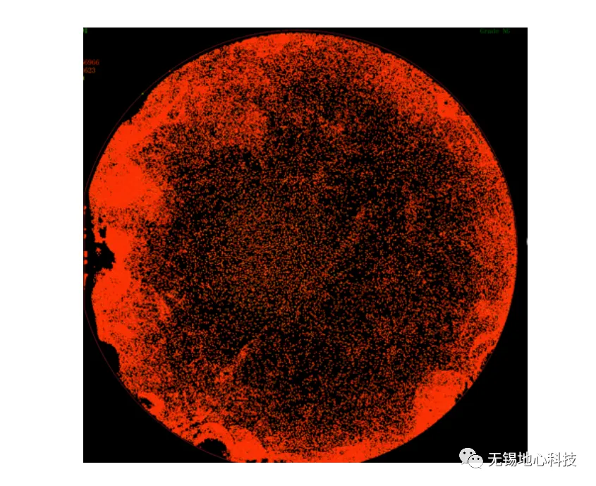
Poor imaging quality in the wafer centre due to defocus
"To maintain overall inspection system performance, the XY scanning stage must have excellent accuracy and flatness. Otherwise, poor stage flatness itself introduces significant focus errors. During high‑speed Y‑axis scanning, the dynamic following error must be sufficiently small; otherwise, Y‑axis‑based trigger signals will be inaccurate.
The Z‑axis requires high accuracy and dynamic performance, including minimal following error and high no‑load cutoff frequency, enabling continuous real‑time focusing within extremely short time frames. Furthermore, every time the wafer enters and exits the optical field of view, the system turns auto‑focus on and off, so the Z‑axis must have sufficient rigidity to minimise overshoot and settle quickly after overshoot."
Achieving rapid auto‑focus tracking during high‑speed wafer defect inspection is a considerable challenge for the motion system.
04 Coretech Solutions
As outlined above, Coretech provides its answer to the rapid auto‑focus tracking challenge in wafer inspection.
By using a linear‑motor‑driven mechanical stage as the XY axes—with the X‑axis stepping and the Y‑axis scanning to trigger the inspection system—paired with a linear‑motor‑driven Z‑lift stage for dynamic focus tracking, and combined with Coretech's proprietary motion control algorithms, this task is accomplished seamlessly.
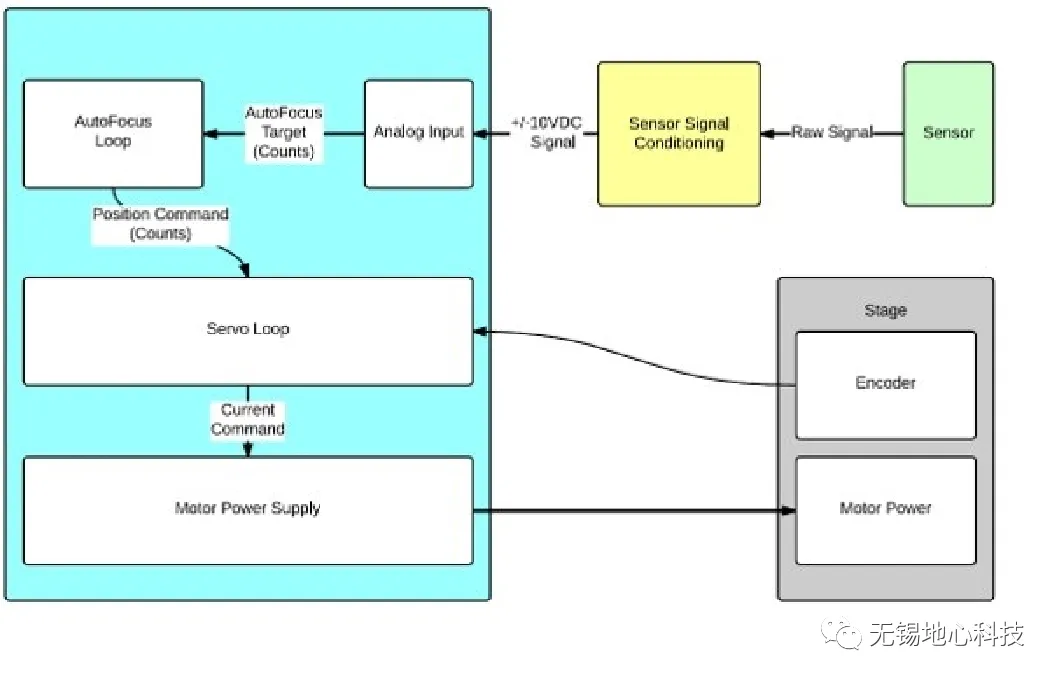
Auto‑focus principle
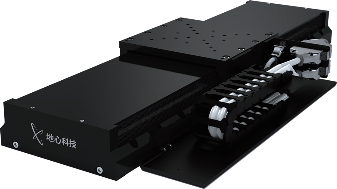
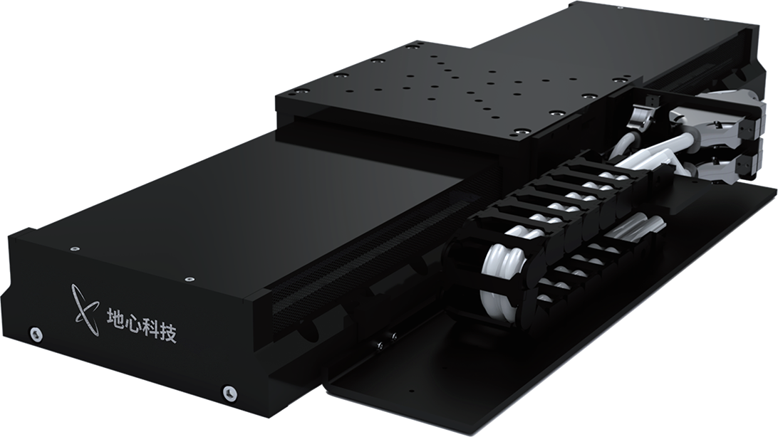
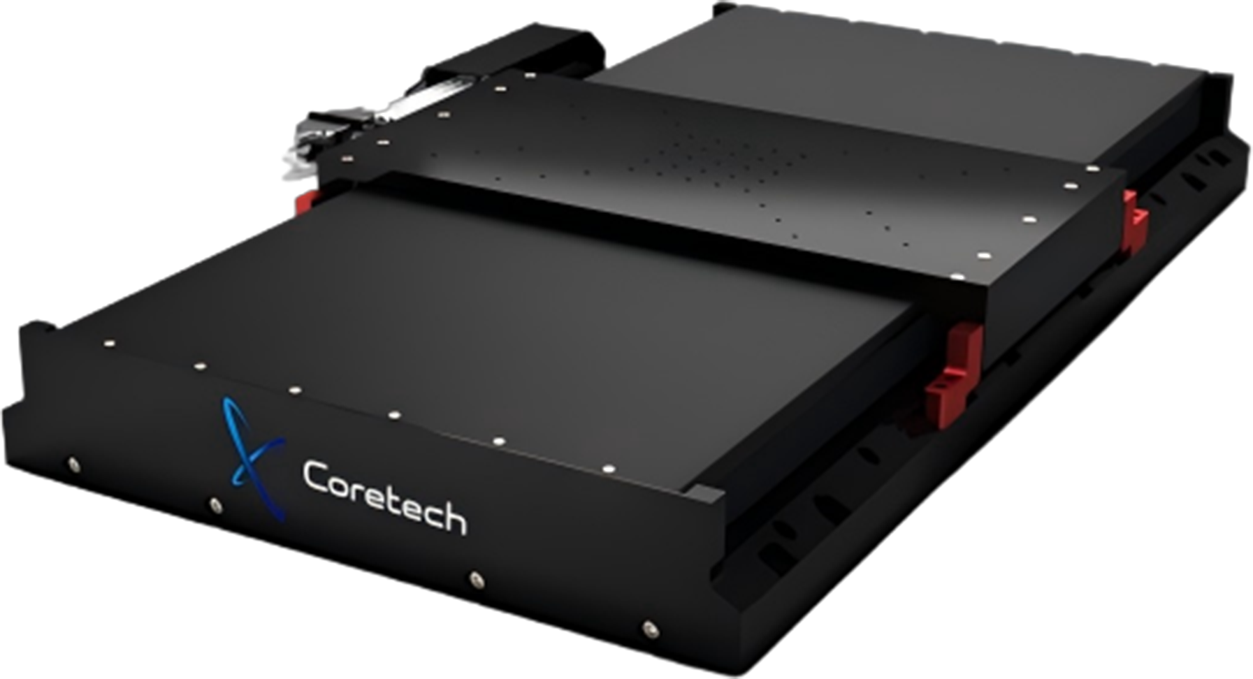
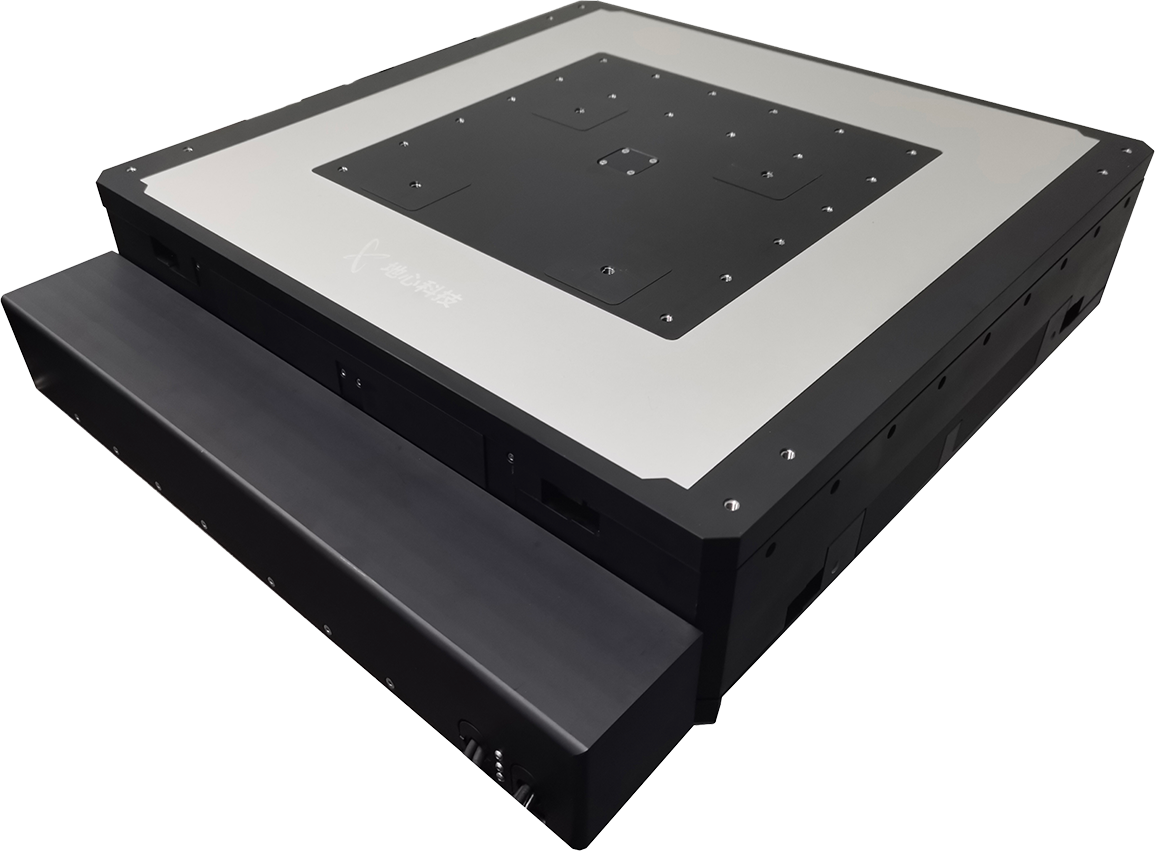
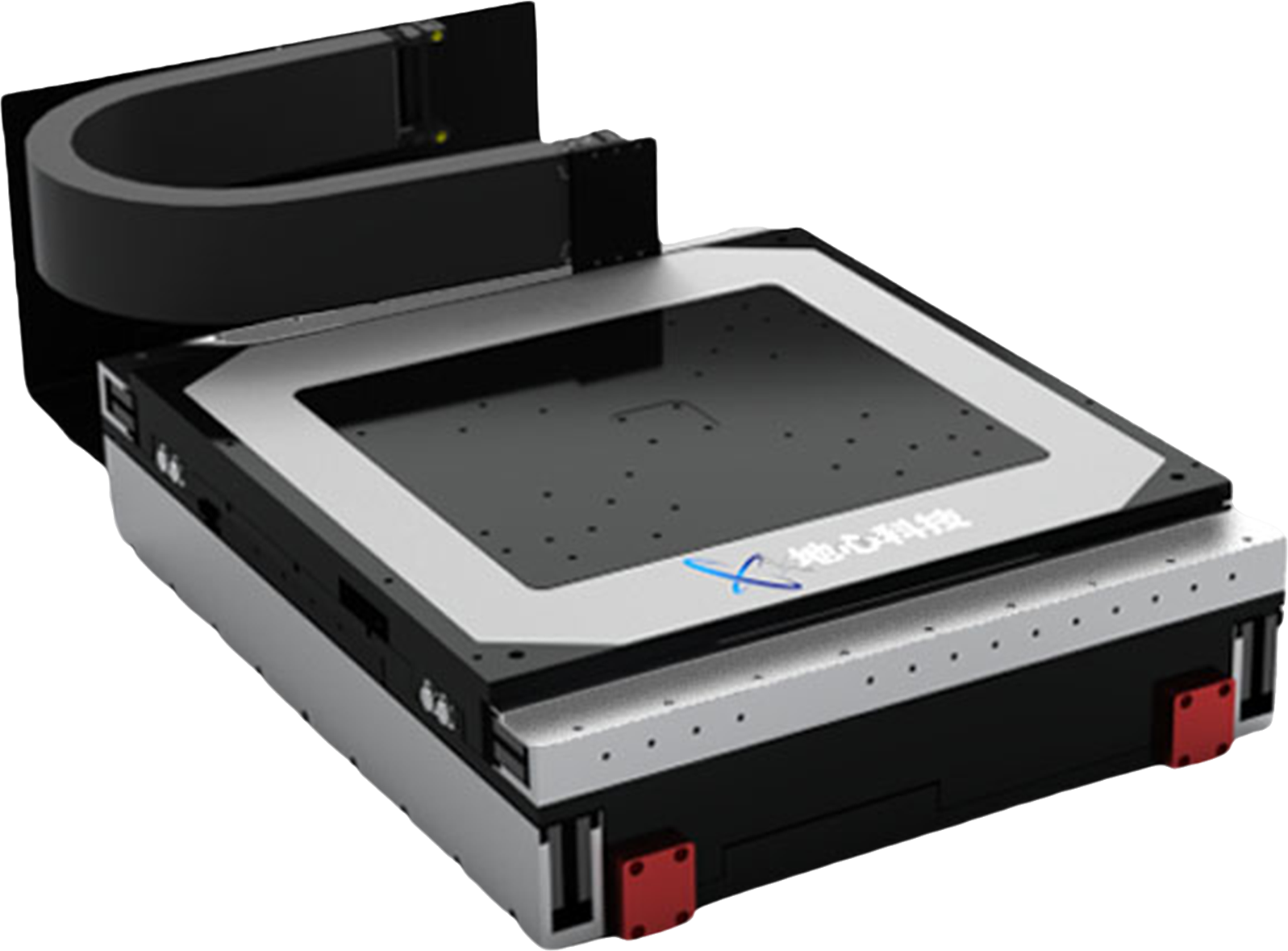
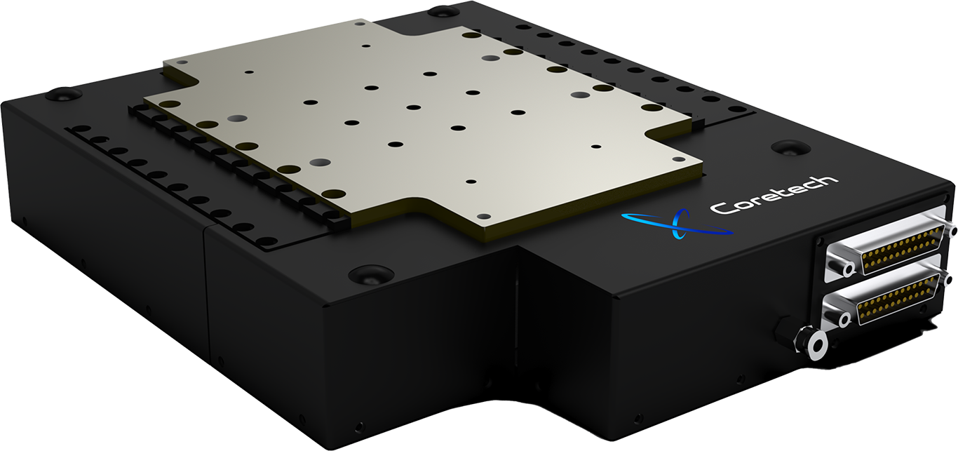
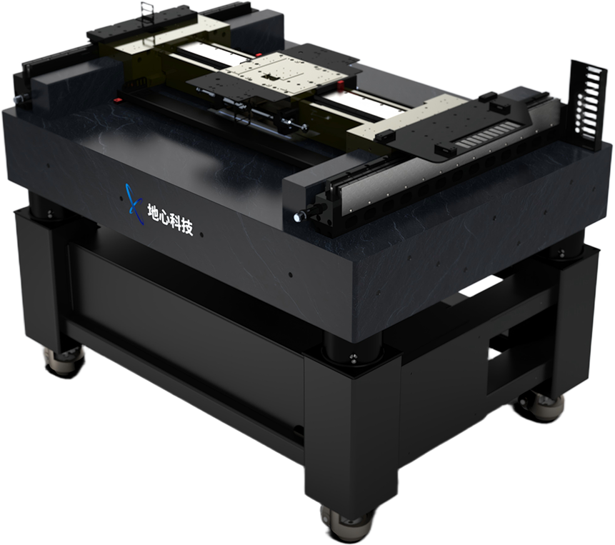
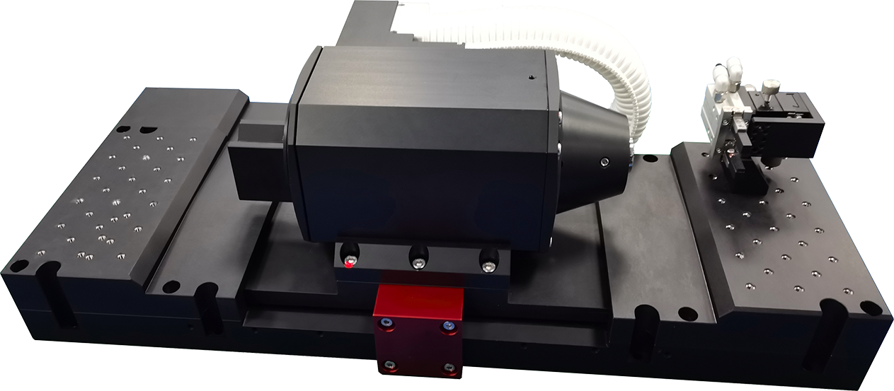
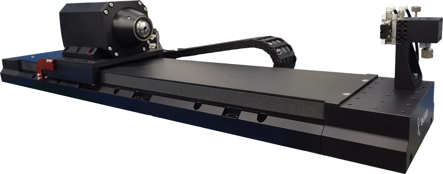
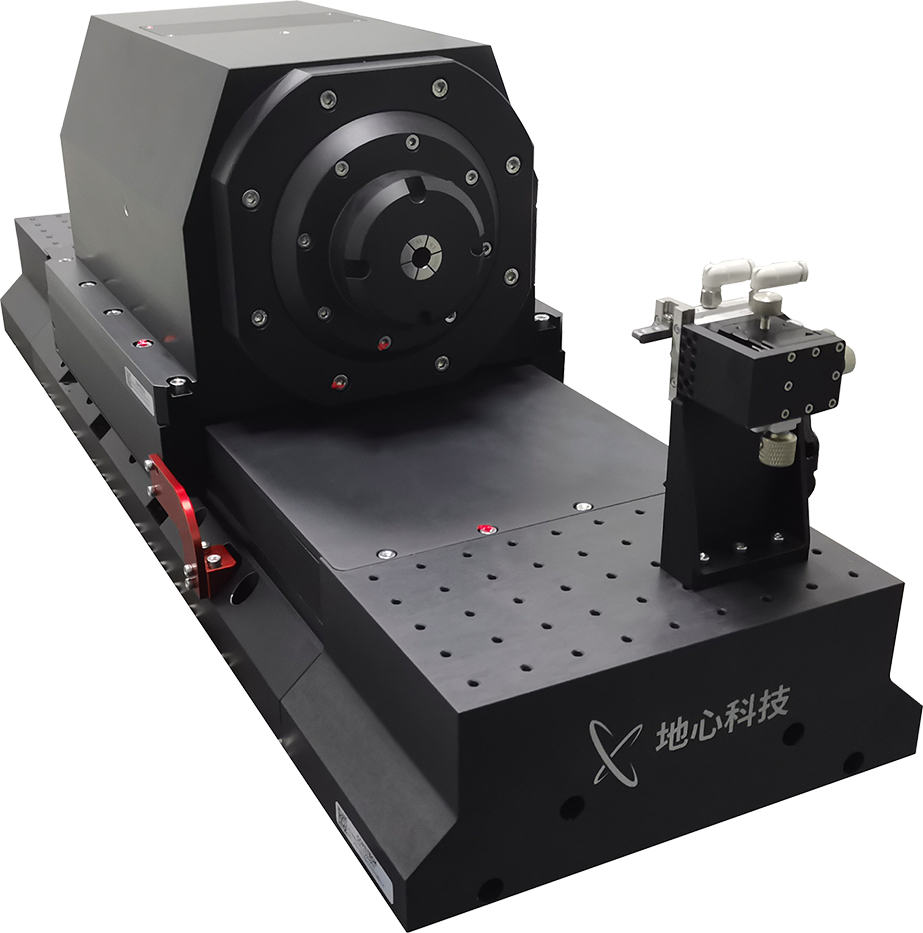
One of Coretech's classic solutions employs the ONEXY‑350‑350 open‑frame XY integrated stage, paired with the SurfaceZ Z‑lift stage. For a 6‑inch or 8‑inch wafer, the wafer is vacuum‑chucked onto the stage surface. The X‑axis performs step motions, while the Y‑axis executes raster‑type scanning. Using position‑based triggering (PEG/PSO) from the controller, image sensors can be triggered at intervals as small as 1 μm or even less, enabling easy scanning inspection. The Z‑lift stage compensates for wafer height variations in real time, keeping the wafer within the camera's focal range.
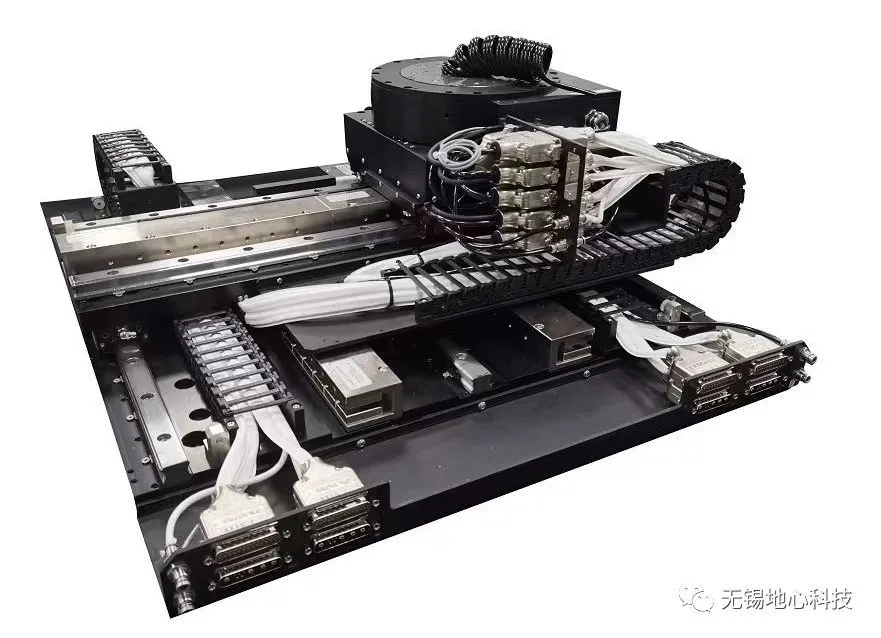
ONEXY‑350‑350 with SurfaceZ auto‑focus solution
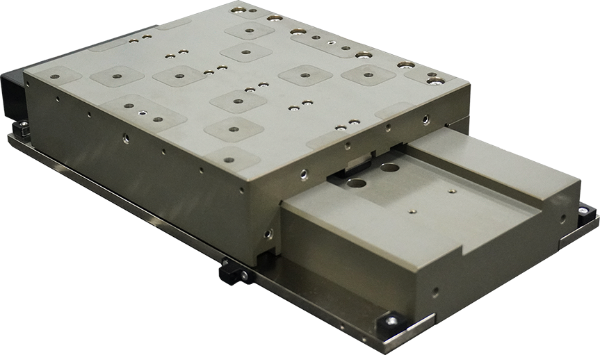
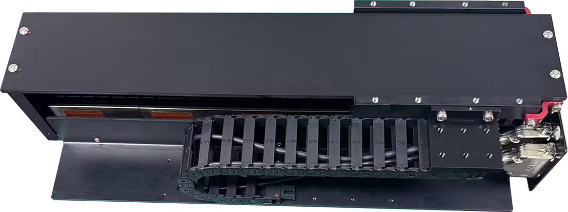
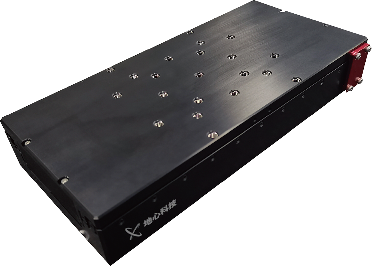
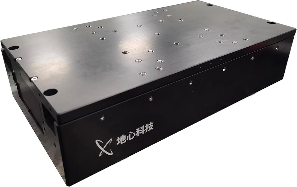
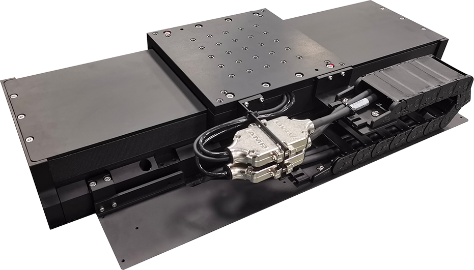
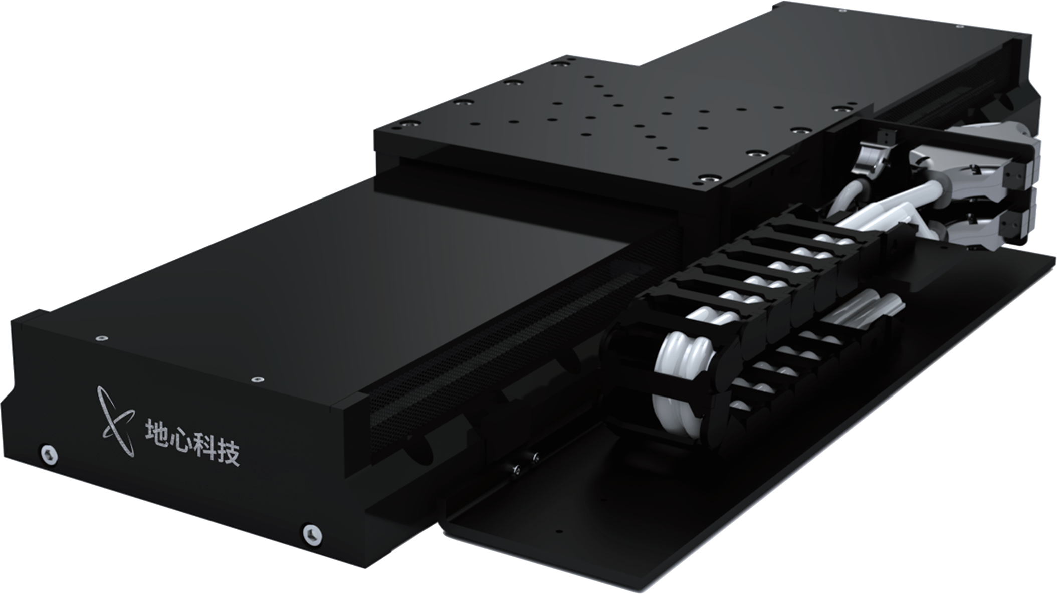
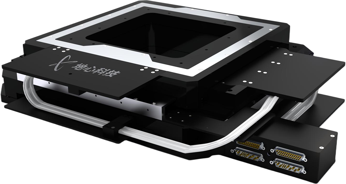
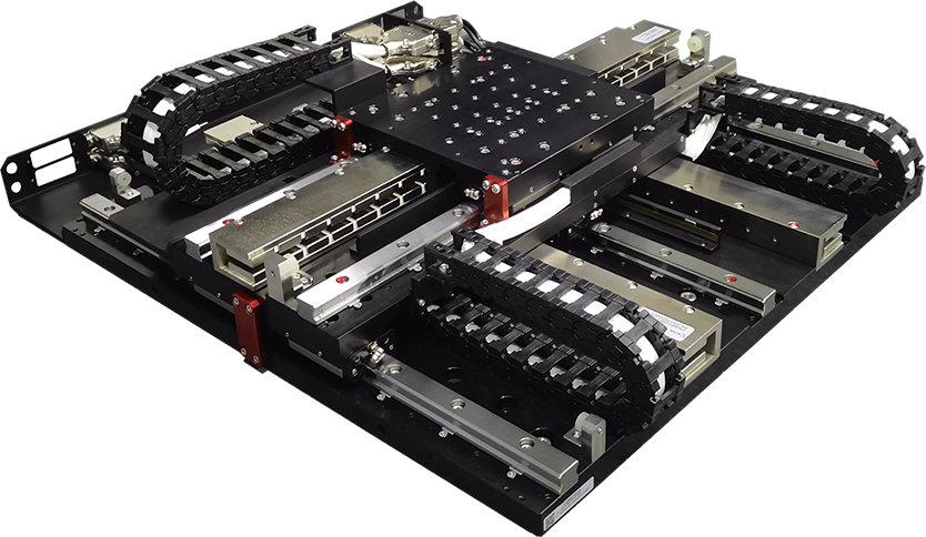
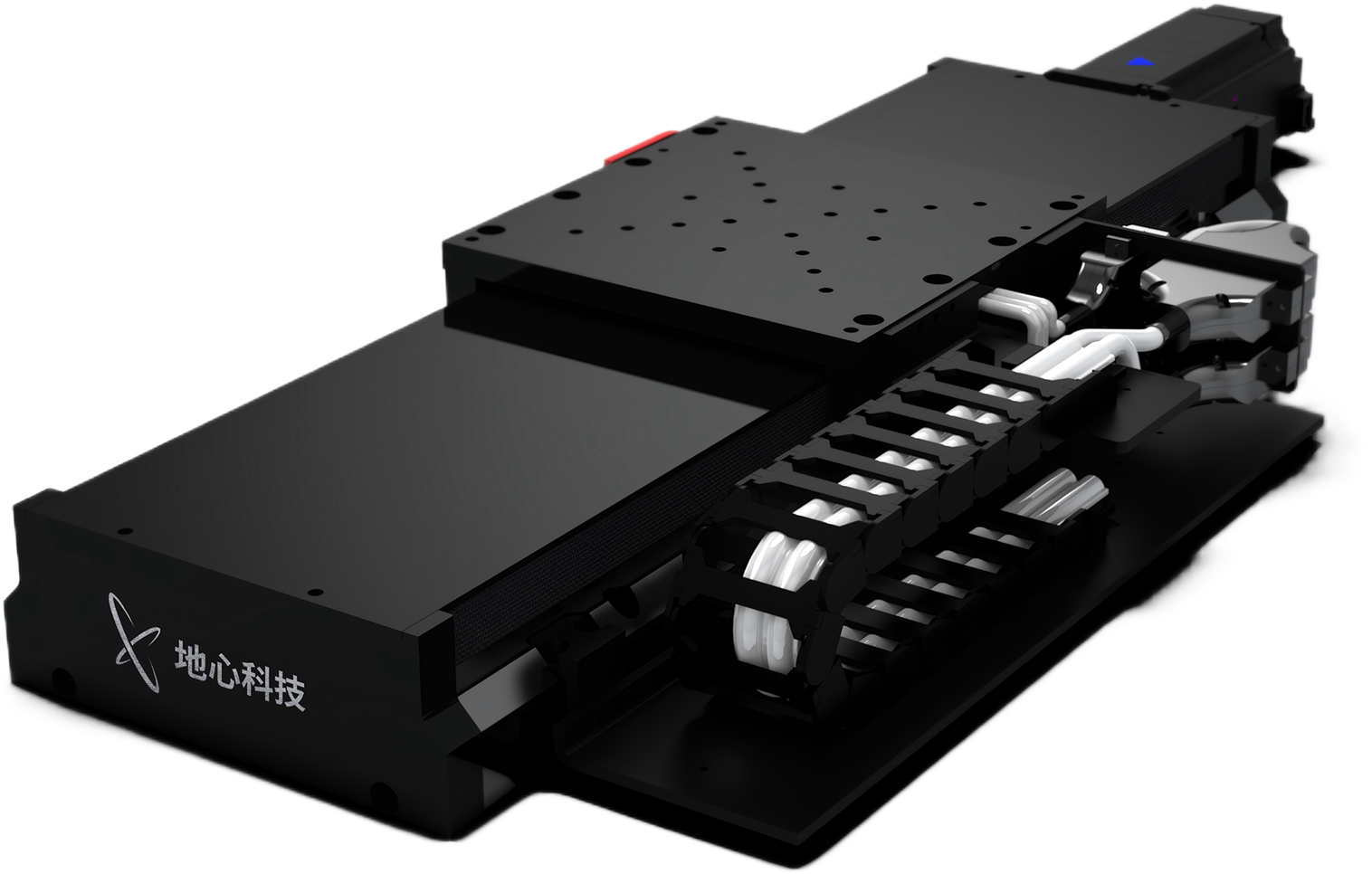
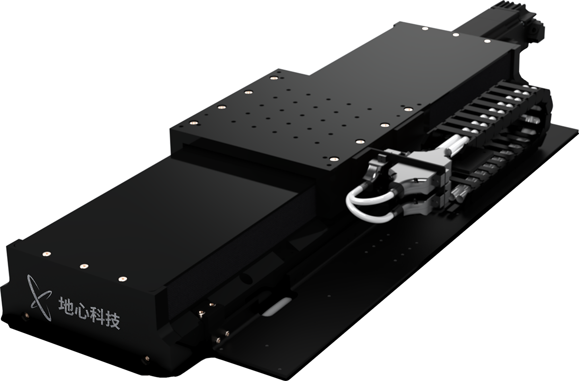
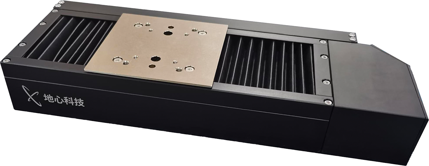
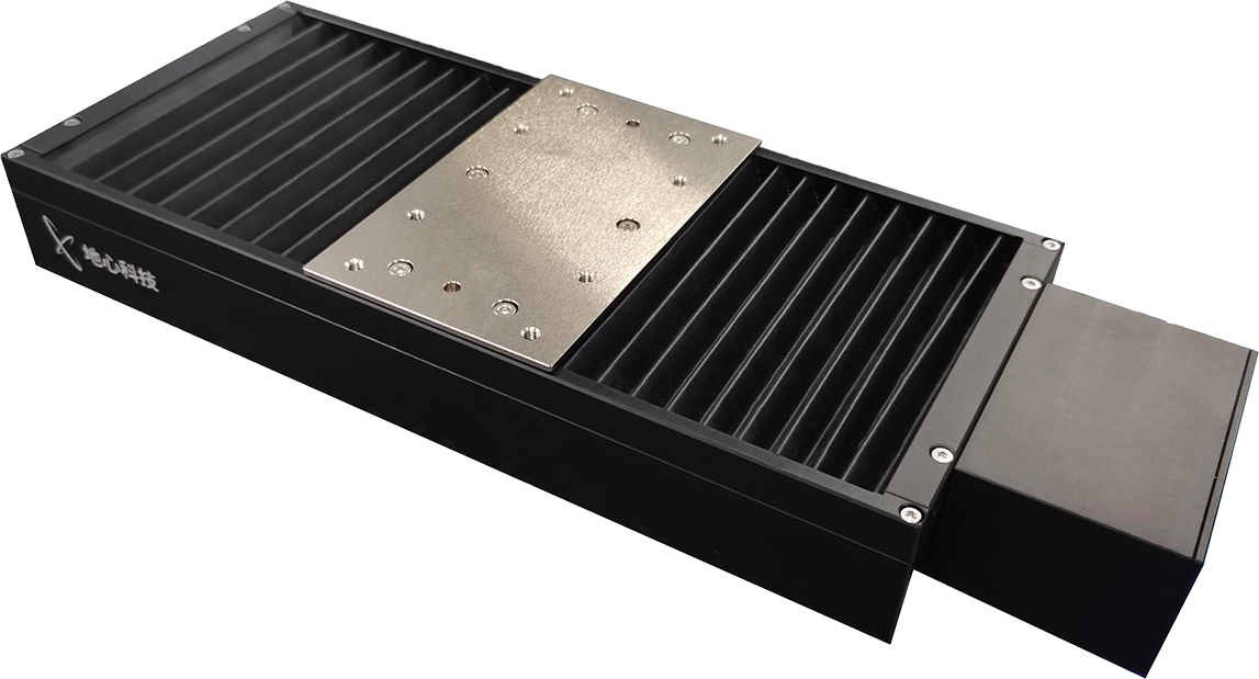
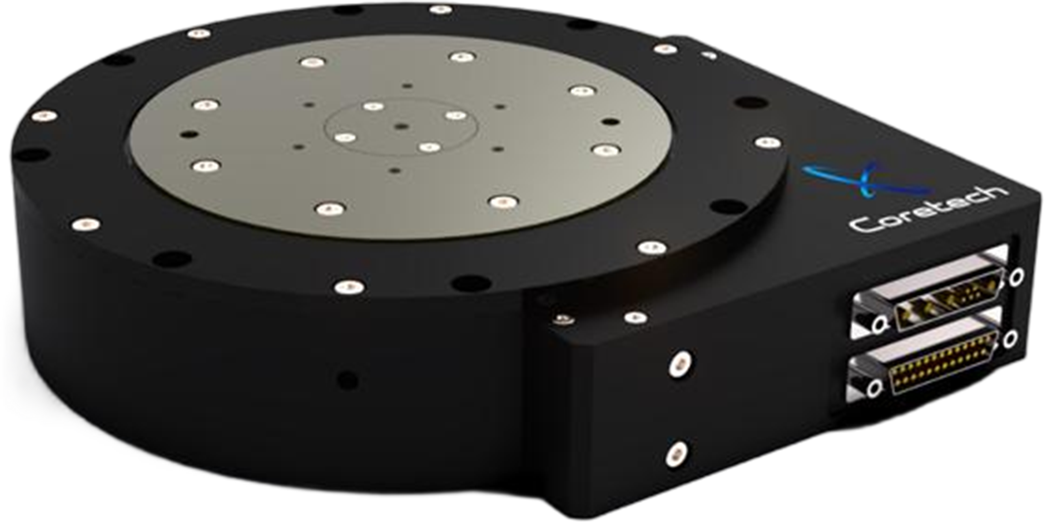
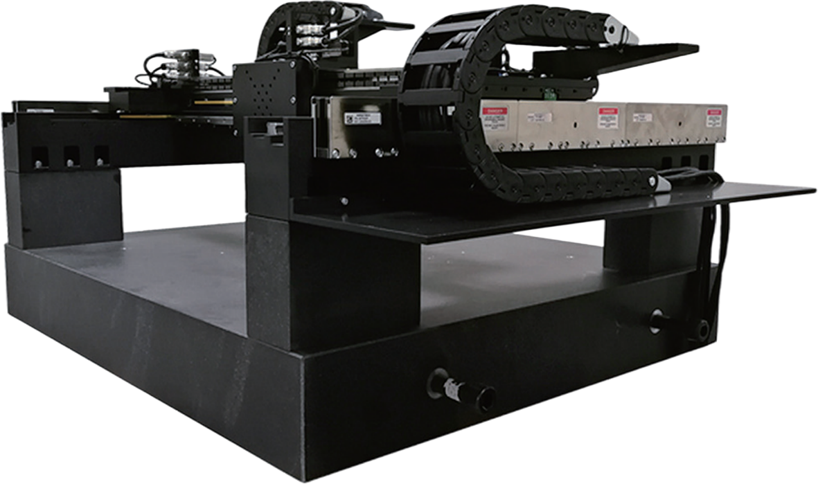
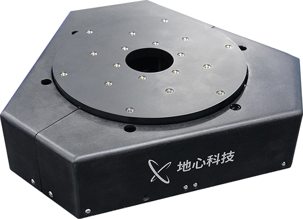
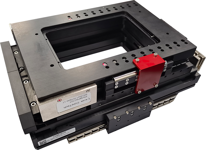
The XY axes utilise Coretech's ONEXY series high‑precision integrated XY motion stage. The ONEXY series employs Coretech's self‑developed direct‑drive motors, with an open‑frame structure and integrated XY design. The lower axis features dual‑motor drive for excellent dynamic performance, superior geometric performance, and higher load capacity. With low lateral height and reduced Abbe error, travel ranges up to 500 mm × 500 mm are available, along with multiple feedback options (including zero‑expansion grating scales). Its outstanding mechanical performance makes it ideal for wafer defect inspection applications.
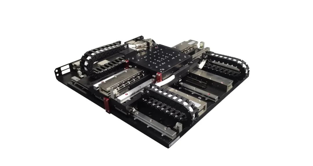
ONEXY‑350‑350 integrated XY motion stage
| 有效行程: | 350*350mm; |
| 双向重复定位误差: | ≤±0.2um; |
| 平面度: | ≤±2.5um; |
| 最大速度: | 2000mm/s |
| 最大负载: | 45kg; |
| 侧面高度: | 115mm; |
| 在位稳定性: | ≤±10nm; |
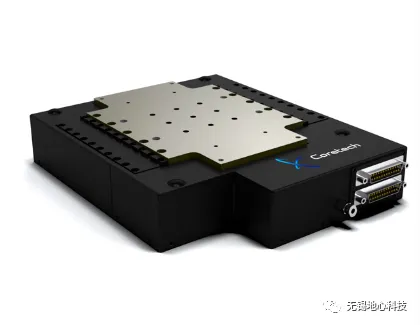
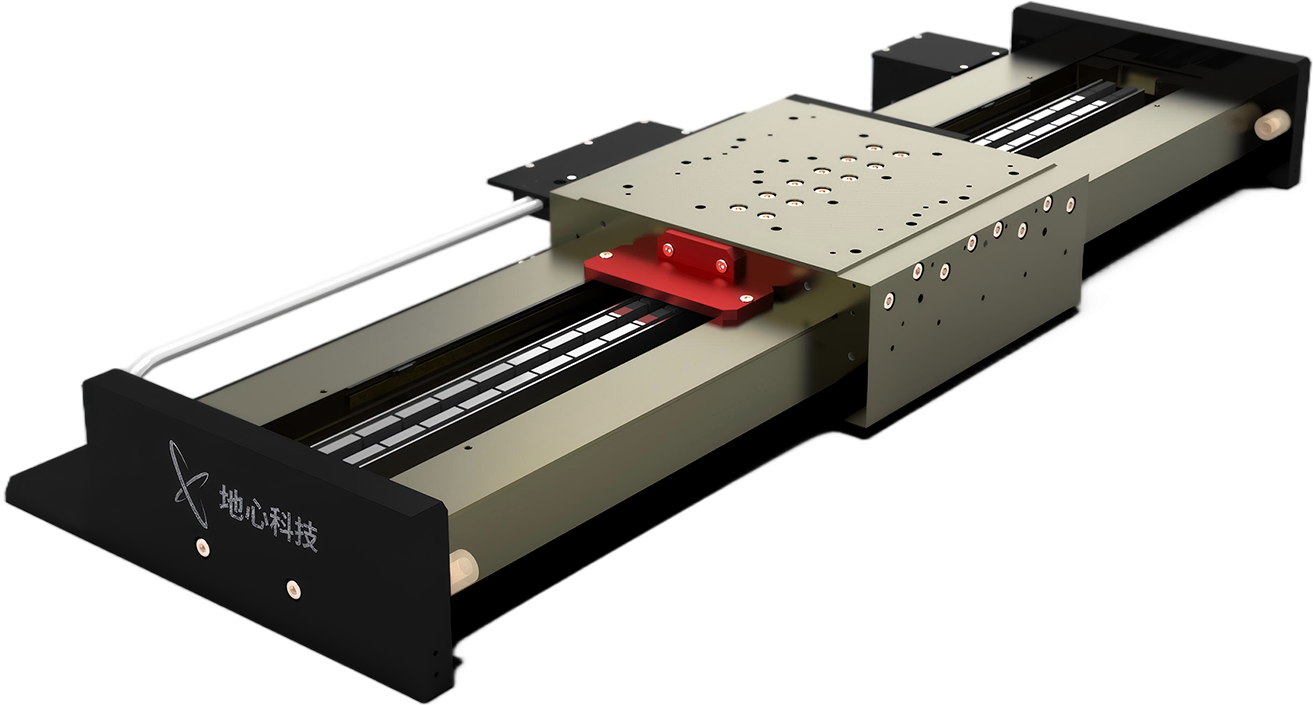
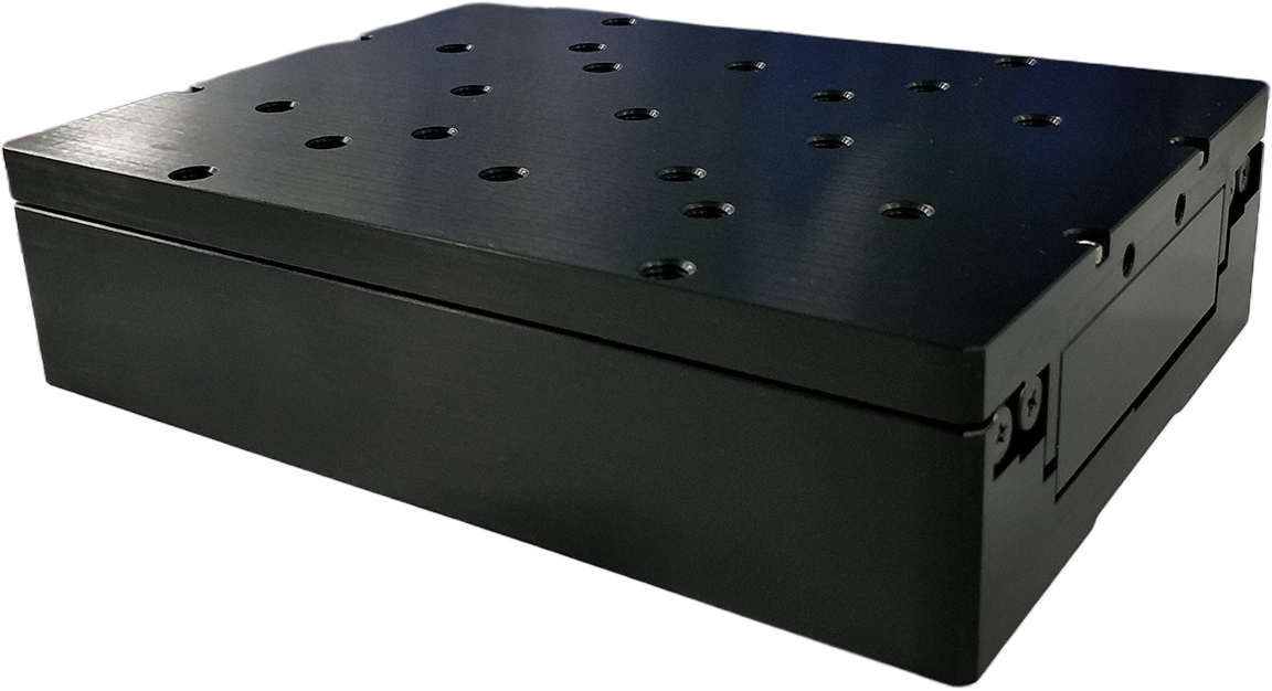
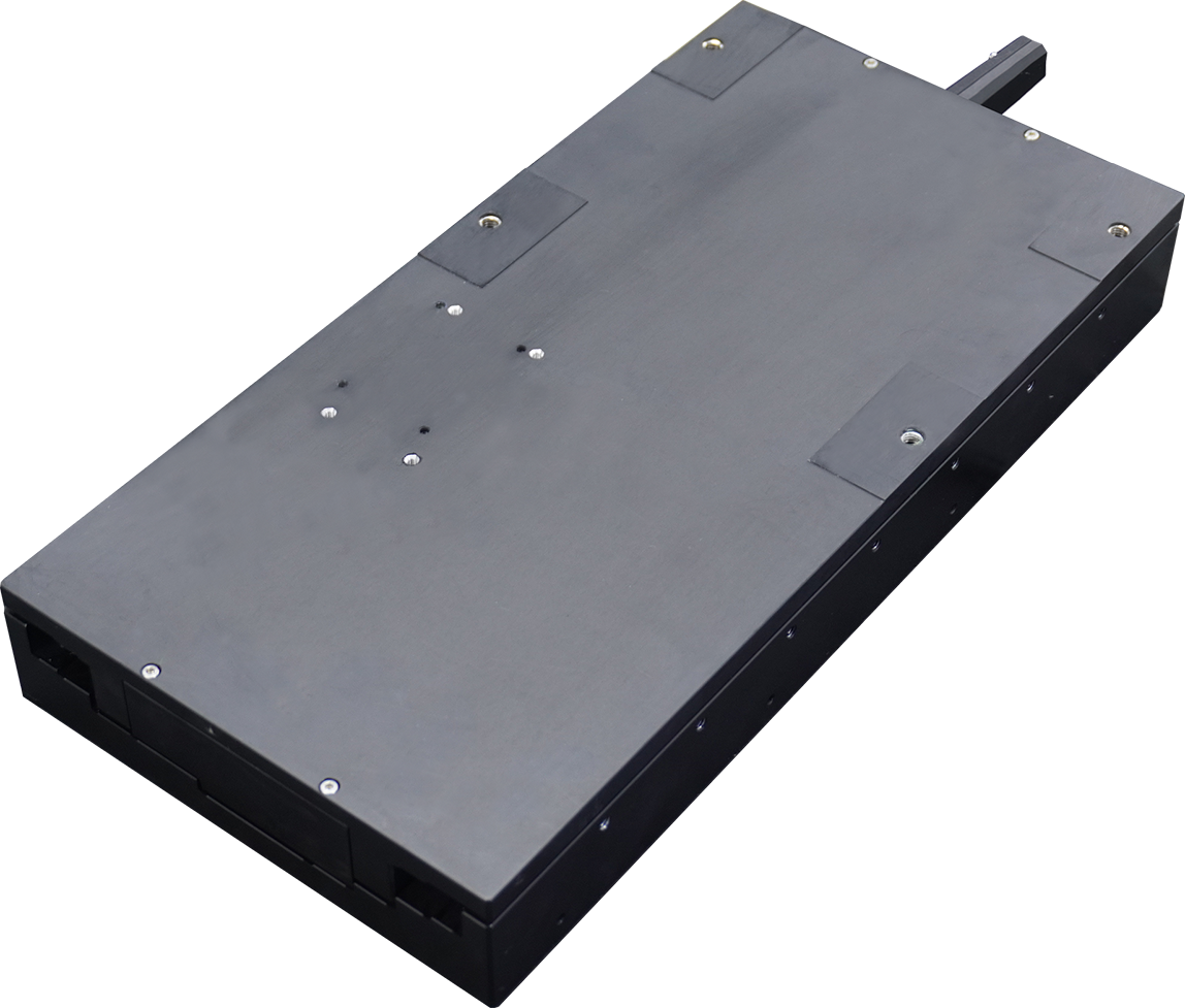
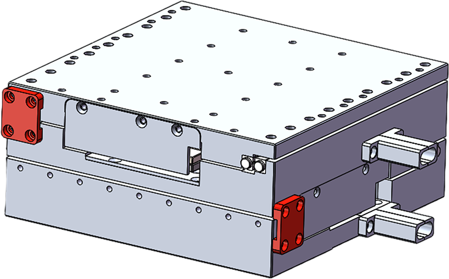
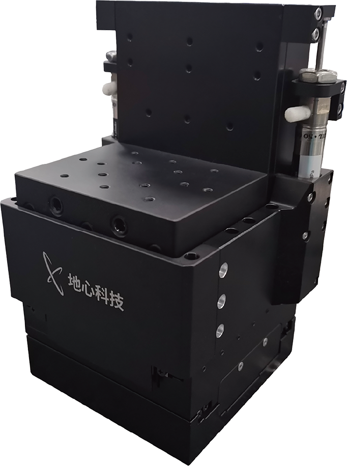
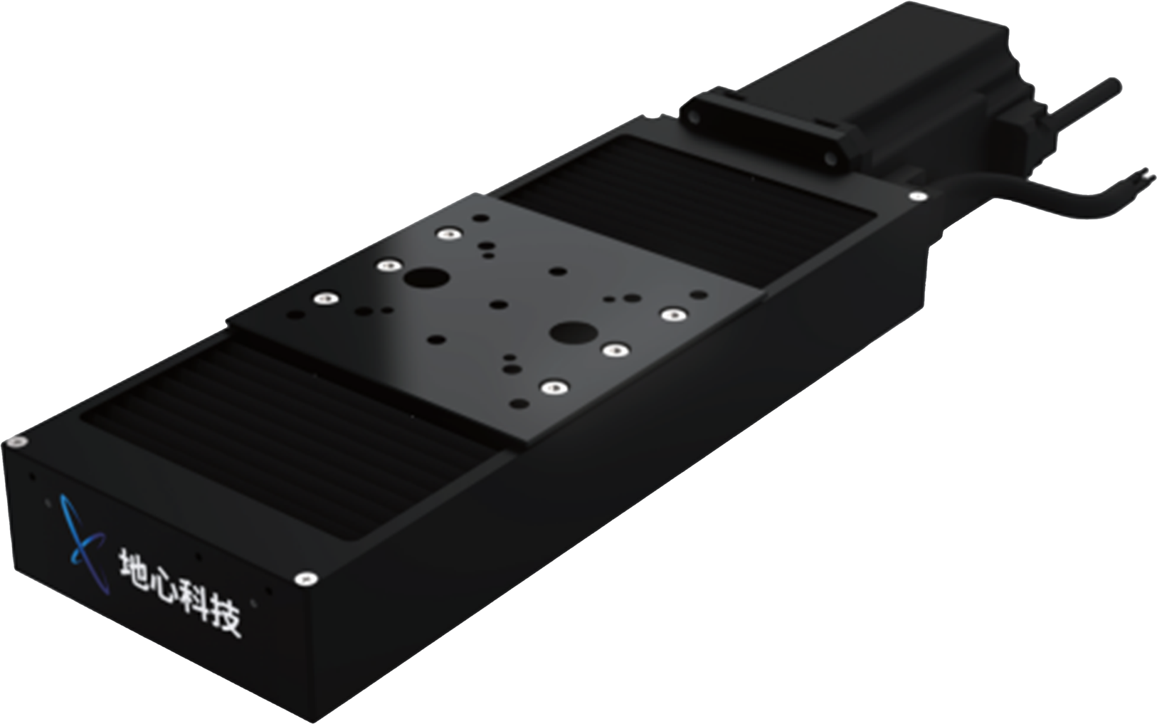
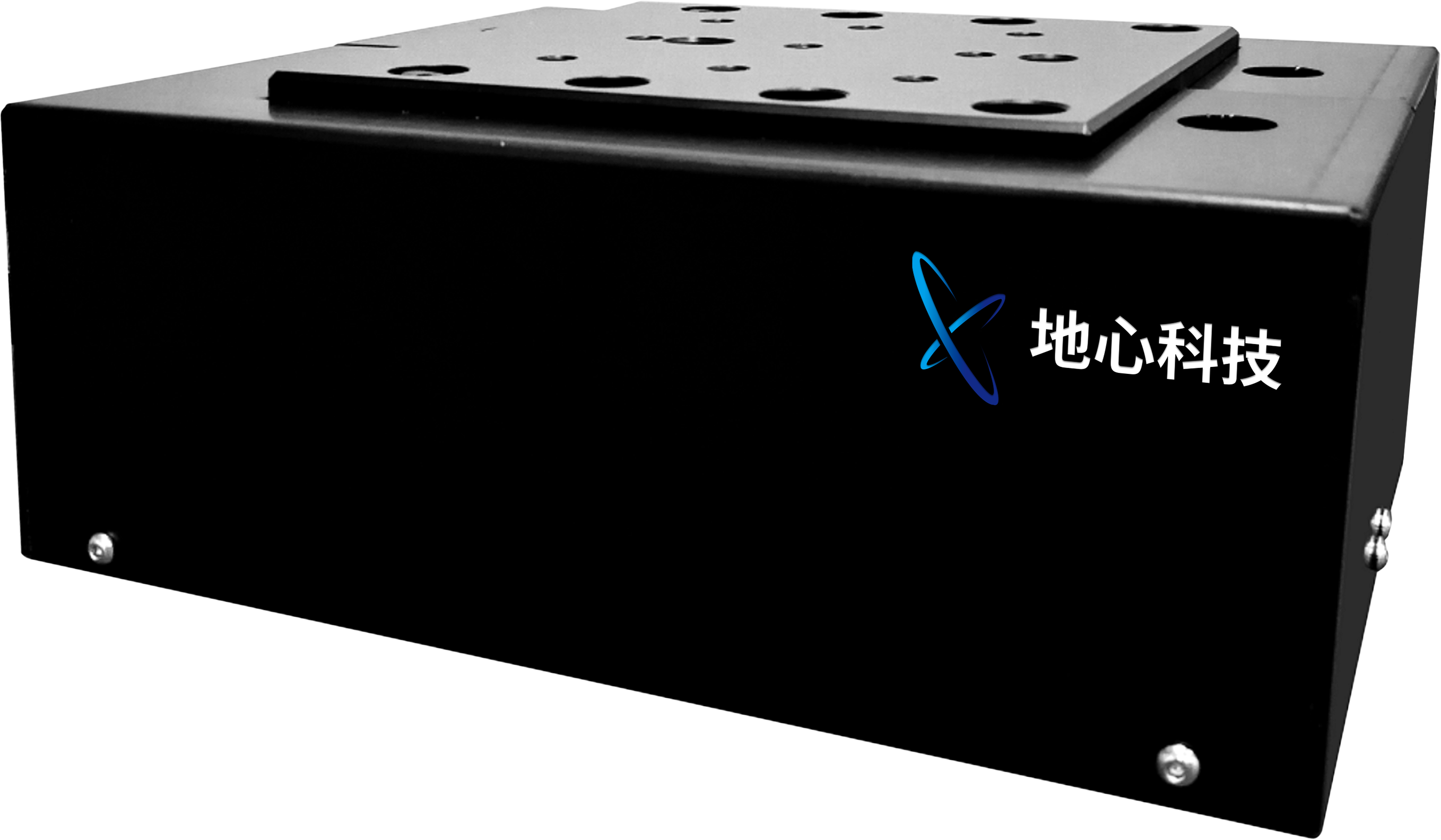
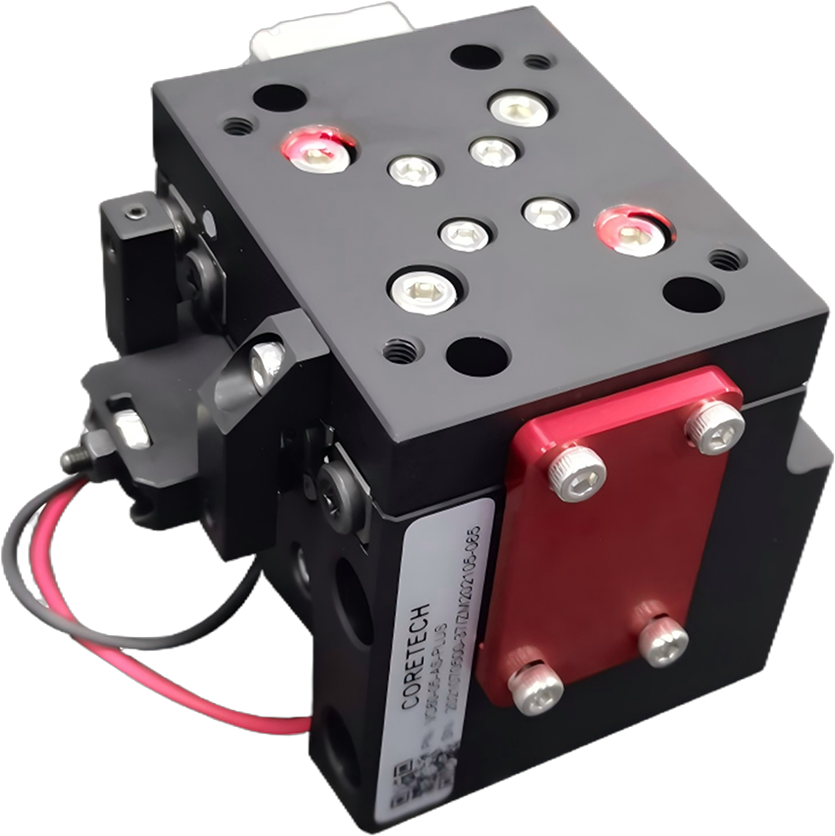
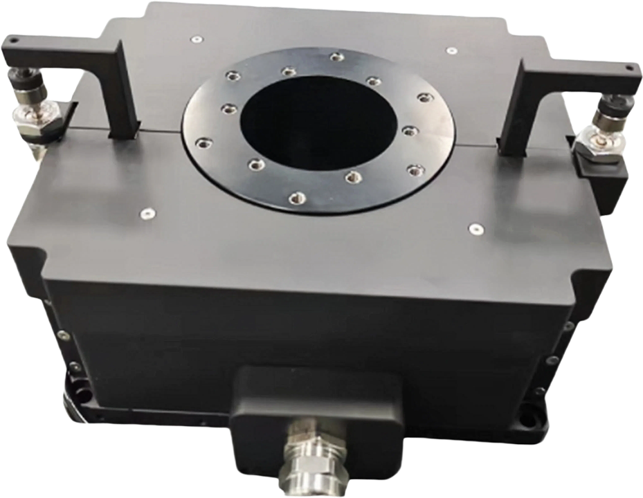
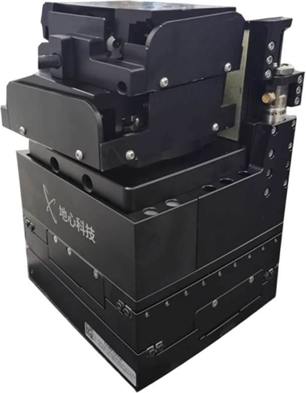
SurfaceZ high‑precision direct‑drive Z‑lift stage
| 有效行程: | 5mm |
| 双向重复定位误差: | ≤±0.1μm |
| 空载截止频率: | ≥200Hz |
| 最大速度: | 5mm/s |
| 在位稳定性: | 5nm |
| 最小步进量: | 5nm |
05 Auto‑Focus Tracking Performance
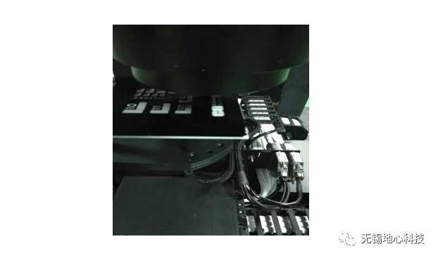
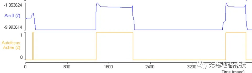
Z‑axis real‑time focus tracking
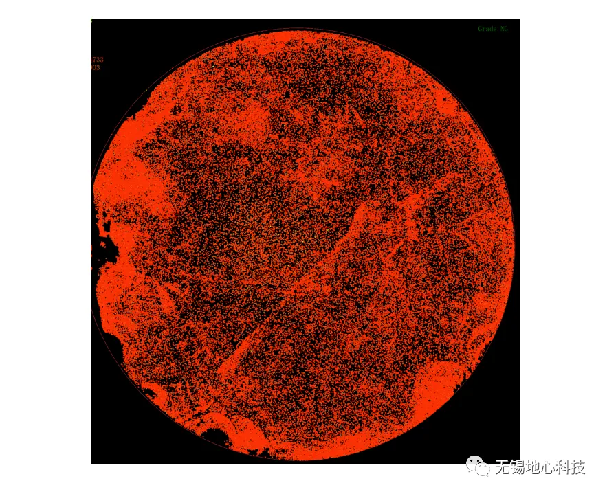
Wafer inspection results with auto‑focus enabled

Comparison of wafer inspection results before and after enabling auto‑focus
If required, we can also provide user‑friendly software tools. With simple configuration, users can generate motion paths, read feedback sensors, implement auto‑focus, and automatically generate corresponding trigger points as required. Additionally, we offer a software development kit (SDK), enabling users to easily integrate the entire system into their own measurement systems—building their custom inspection solutions quickly and reliably.
Featured News
Laser Processing Automation Solutions – PCB Drilling
2026.06.03
One Article Summary | Multiple Applications of Precision Motion Stages in Wafer Defect Inspection
2026.06.03
A Comprehensive Overview of the HBM Manufacturing Process: What Role Does the High-Precision Motion Platform Play?
2026.06.03
 Back to List