
.png)

.png)







Home
 News Center
Behind the Mass Production of Hybrid Bonding: How Precision Motion Stages Meet the High-Precision Control Demands of Semiconductor Packaging
News Center
Behind the Mass Production of Hybrid Bonding: How Precision Motion Stages Meet the High-Precision Control Demands of Semiconductor Packaging
News Center
Behind the Mass Production of Hybrid Bonding: How Precision Motion Stages Meet the High-Precision Control Demands of Semiconductor Packaging
Behind the Mass Production of Hybrid Bonding: How Precision Motion Stages Meet the High-Precision Control Demands of Semiconductor Packaging
 2026-06-02
Share:


As the semiconductor industry advances toward smaller process nodes, traditional packaging technologies can no longer meet the demands of high-performance chips in terms of integration density, signal transmission, and energy efficiency. Advanced packaging technologies such as Heterogeneous Integration (HI), Chiplet, and System-in-Package (SiP) are increasingly becoming industry focal points, and these technologies impose stringent requirements on packaging accuracy.
01 Industry Background
As Moore's Law slows, advanced packaging is regarded as a key driving force for sustaining chip performance improvements in the post-Moore era.
Recently, the Semiconductor Research Corporation (SRC) released the highly anticipated Microelectronics and Advanced Packaging Technology Roadmap 2.0 (MAPT 2.0). This roadmap systematically outlines the development blueprint for semiconductor packaging technologies over the next decade, indicating that future semiconductor packaging will increasingly rely on advanced packaging technologies such as heterogeneous integration and chiplets.
The core advantage of heterogeneous integration technology lies in its ability to integrate chips of different process nodes, functionalities, and even materials into a single package structure. This achieves system-level performance with high bandwidth, low latency, and low power consumption at the packaging level, while offering greater cost-control flexibility compared to full-function system-on-chip (SoC) solutions.
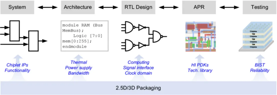
Figure 1: Chip-package co-design workflow
If heterogeneous integration can be likened to constructing a fully functional skyscraper, then hybrid bonding is the most advanced and robust steel-rebar connection technology within it. Among the many advanced packaging processes, hybrid bonding demonstrates significant advantages due to its ability to deliver extreme interconnect density, higher transmission bandwidth, superior energy efficiency, and a more compact system footprint.
02 Technical Requirements
Hybrid bonding technology is progressively moving toward industrial-scale applications and currently stands on the brink of a manufacturing ramp-up.
In 2015, Sony pioneered the mass production of hybrid bonding technology in its CMOS image sensors. In 2022, AMD launched its first vertically-cached gaming processor, the Ryzen 7 5800X3D. The most distinctive feature of this processor is the addition of a stacked SRAM expansion chip on top of the compute chiplet, expanding the L3 cache from 32 MB to 96 MB.
This design enables the external cache chip to achieve performance nearly equivalent to being directly integrated within the compute chip, demonstrating the critical role of hybrid bonding in high-performance heterogeneous integration.
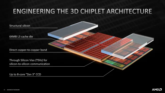
Figure 2: AMD-related products
In July this year, Samsung announced that it would begin applying hybrid bonding technology starting with the 16-layer stack of HBM4E (seventh-generation high-bandwidth memory); SK Hynix plans to introduce hybrid bonding technology starting with the 20-layer stacked HBM4E; and Micron announced in June that it had begun shipping its next-generation HBM4 memory samples to key customers.
As heterogeneous integration technology advances toward higher density and integration of more components, advanced processes such as hybrid bonding are subject to increasingly stringent accuracy requirements. In hybrid interconnect processes with chip-to-wafer bonding pitches of less than 3 μm, the bonding alignment accuracy (3σ) is typically required to be controlled within 10% of the bonding pitch (i.e., when the pitch is <3 μm, the 3σ accuracy must be <0.3 μm).
At the same time, as more components and interconnects are incorporated into a single package, the number of potential failure points increases. A defect in any single chip or interconnect can jeopardize the entire multi-chip package, resulting in costly yield losses. In this environment, tighter process control becomes indispensable for ensuring high yield and high reliability.
Against the backdrop of continuously shrinking bump pitches, increasing integration density, and growing heterogeneity in integration schemes, precision motion stages must achieve further breakthroughs in nanometer-scale positioning accuracy and multi-axis synchronous control to support the demanding requirements of next-generation advanced packaging processes.
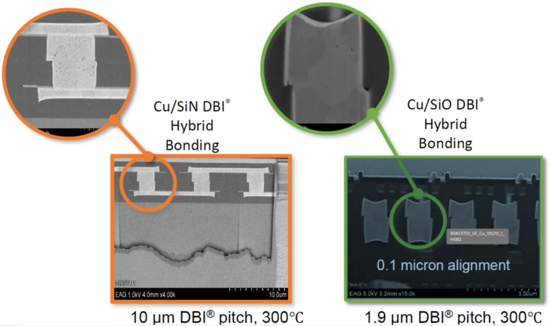
Figure 3: 10 μm-pitch hybrid bonding (left) and 1.9 μm-pitch hybrid bonding (right) by NHanced Semiconductors, Inc.
03 Geocentric Solutions
With an application-driven approach, Geocentric Technology has been deeply engaged in the high-precision motion stage field for many years, accumulating extensive customisation experience in real-world semiconductor industry applications. Addressing the stringent requirements that hybrid bonding imposes on motion stages, Geocentric Technology offers a range of high-precision motion stages precisely tailored to customer W2W/D2W application scenarios:
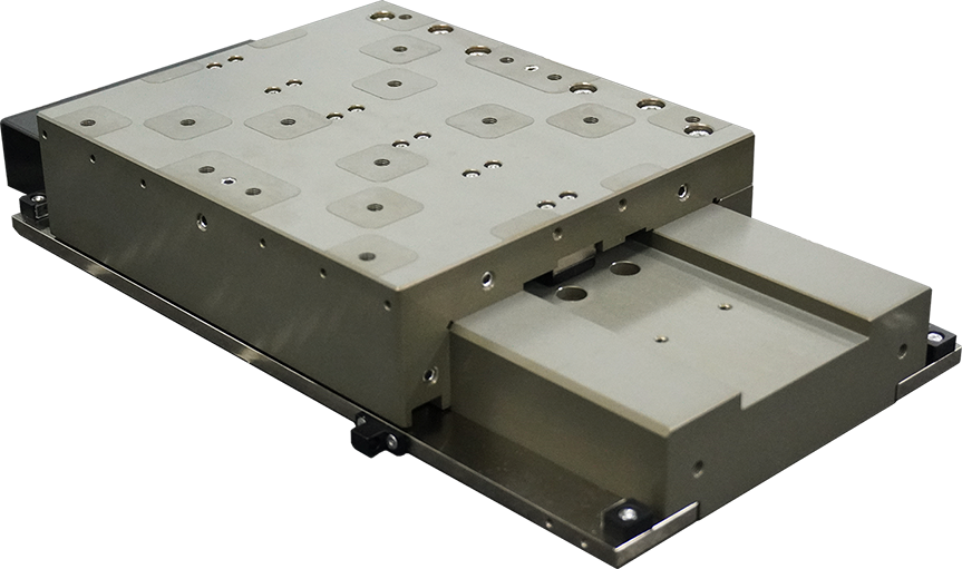
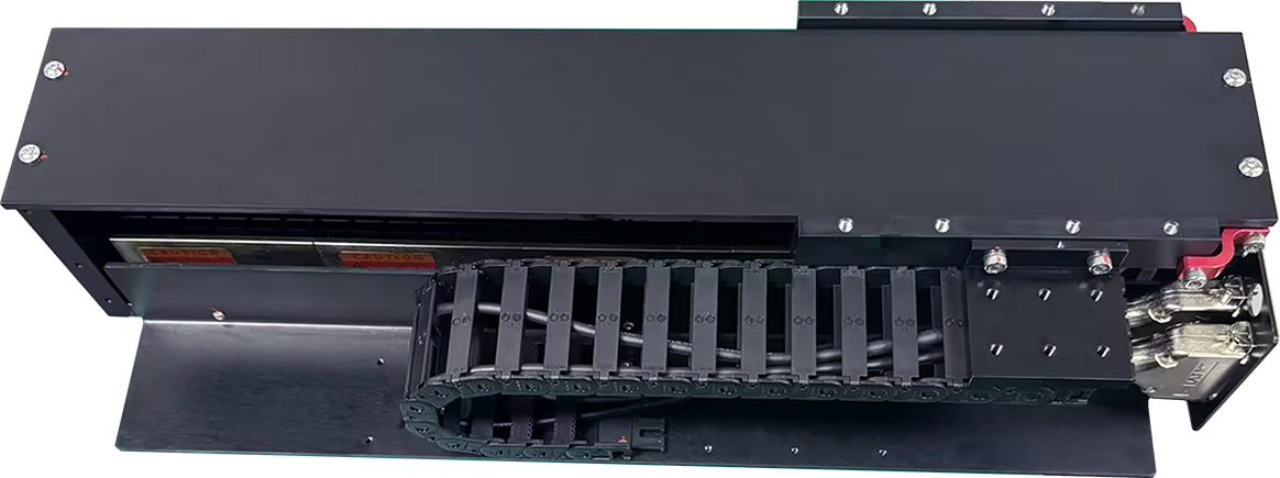
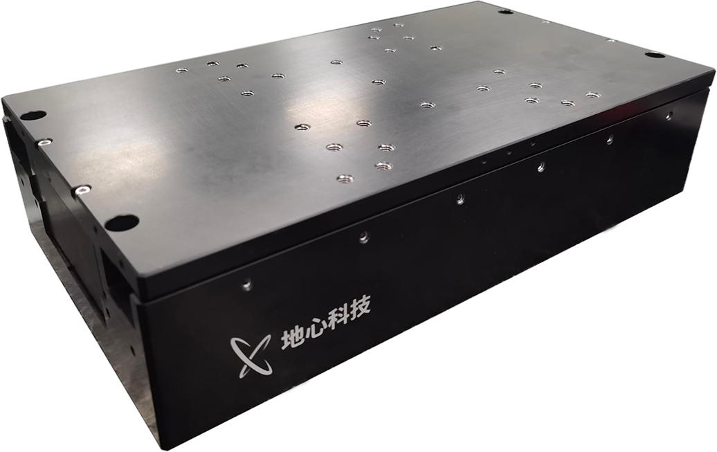
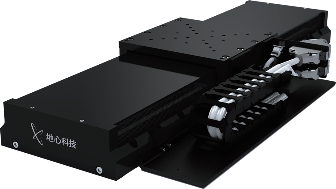
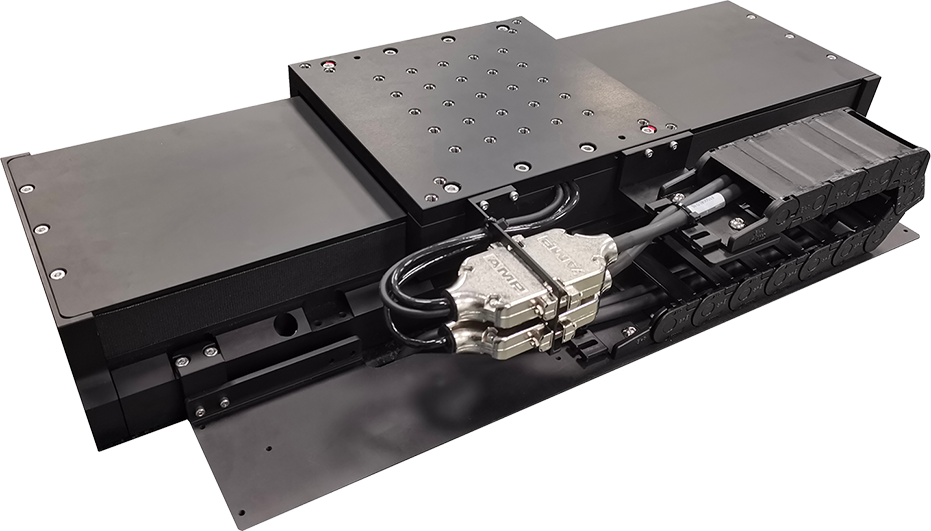
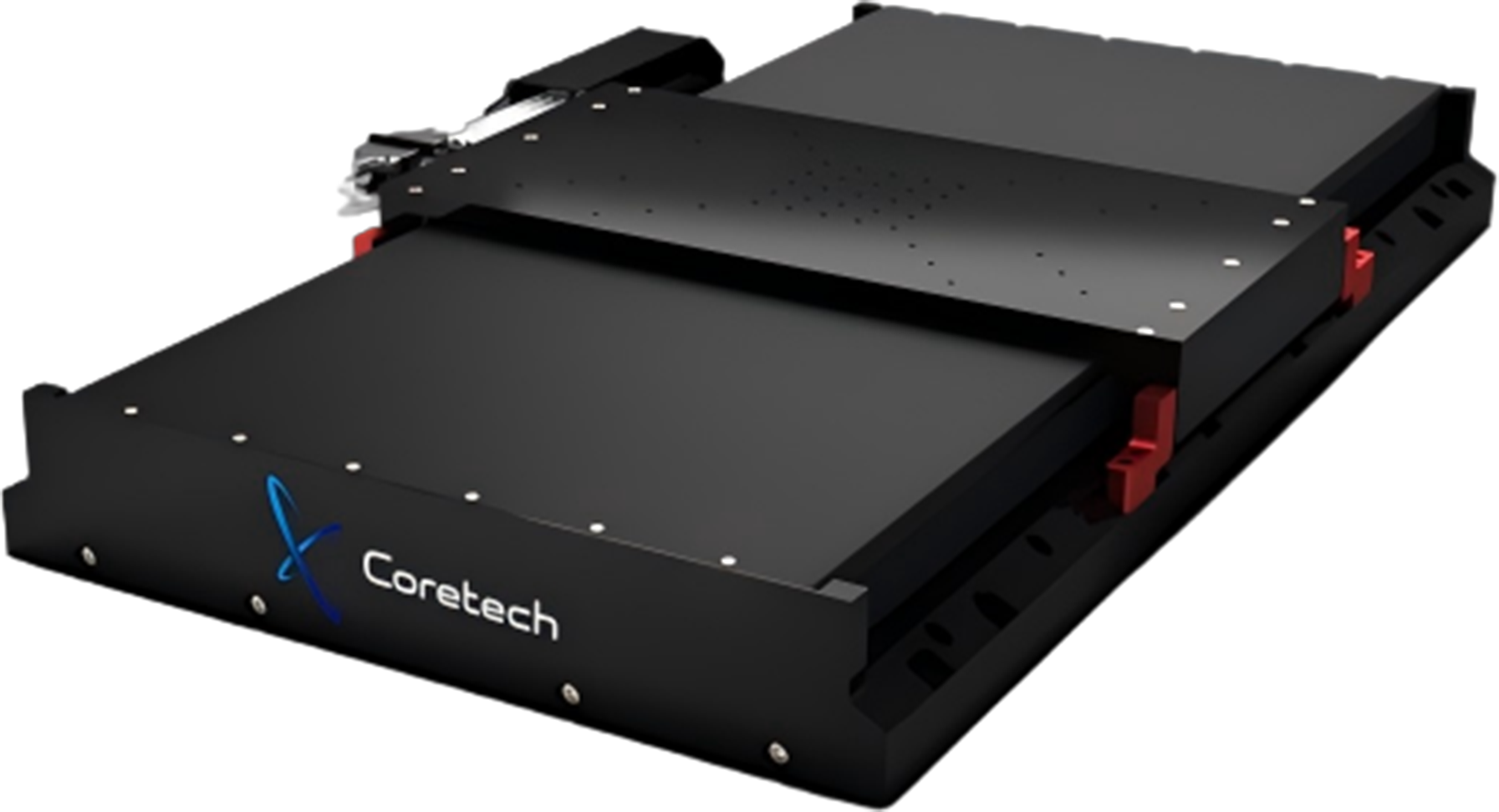
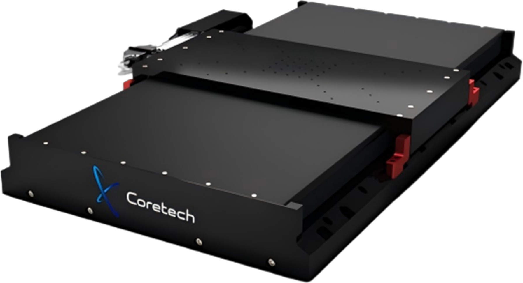
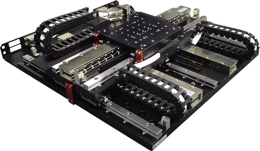
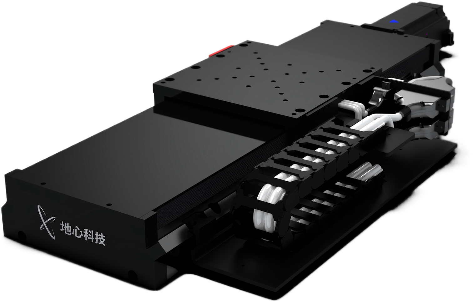
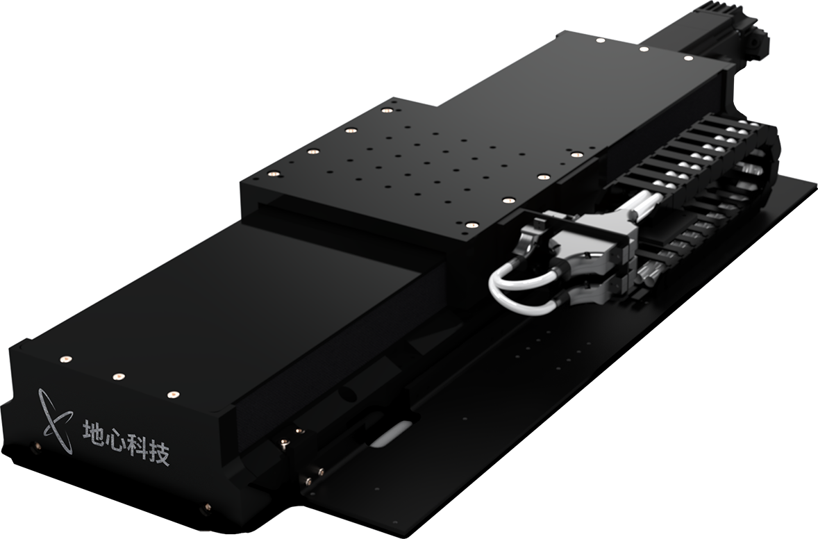
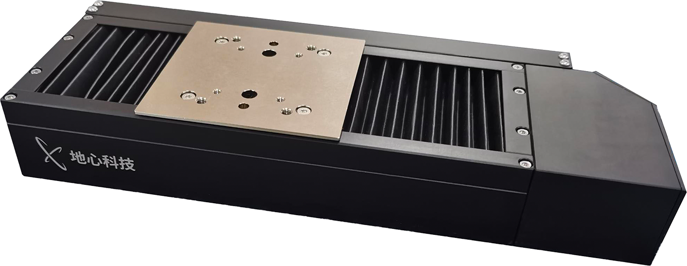
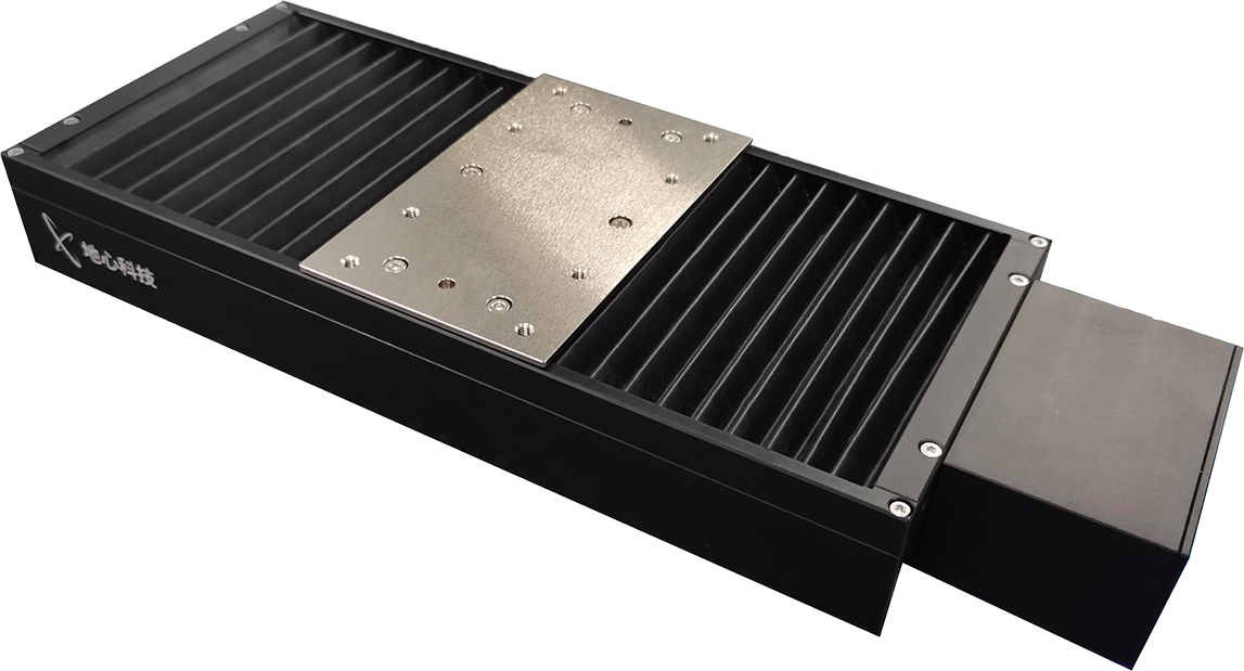
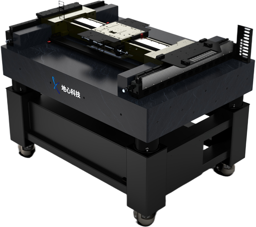
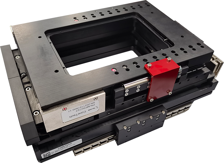
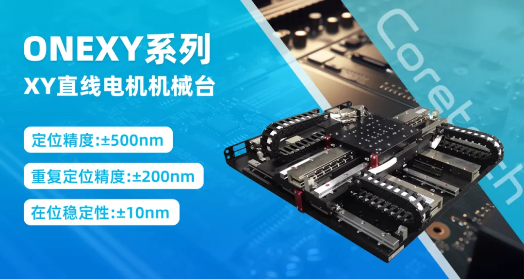
ONEXY Series XY Linear Motor Mechanical Stage
Enables high-precision, high-speed positioning of chips/wafers in the horizontal plane, reducing bonding misalignment caused by positioning errors.
Electronic resolution: 1 nm; minimum step: <20 nm.
Wide range of travel options, combining large stroke, high precision, heavy load capacity, and low lateral height.
Open-frame structure facilitates integration into various multi-axis configurations.
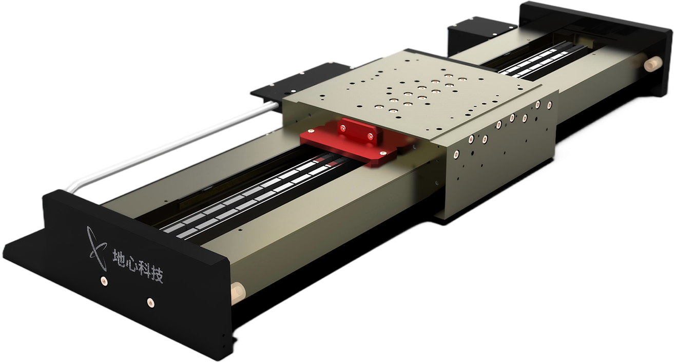
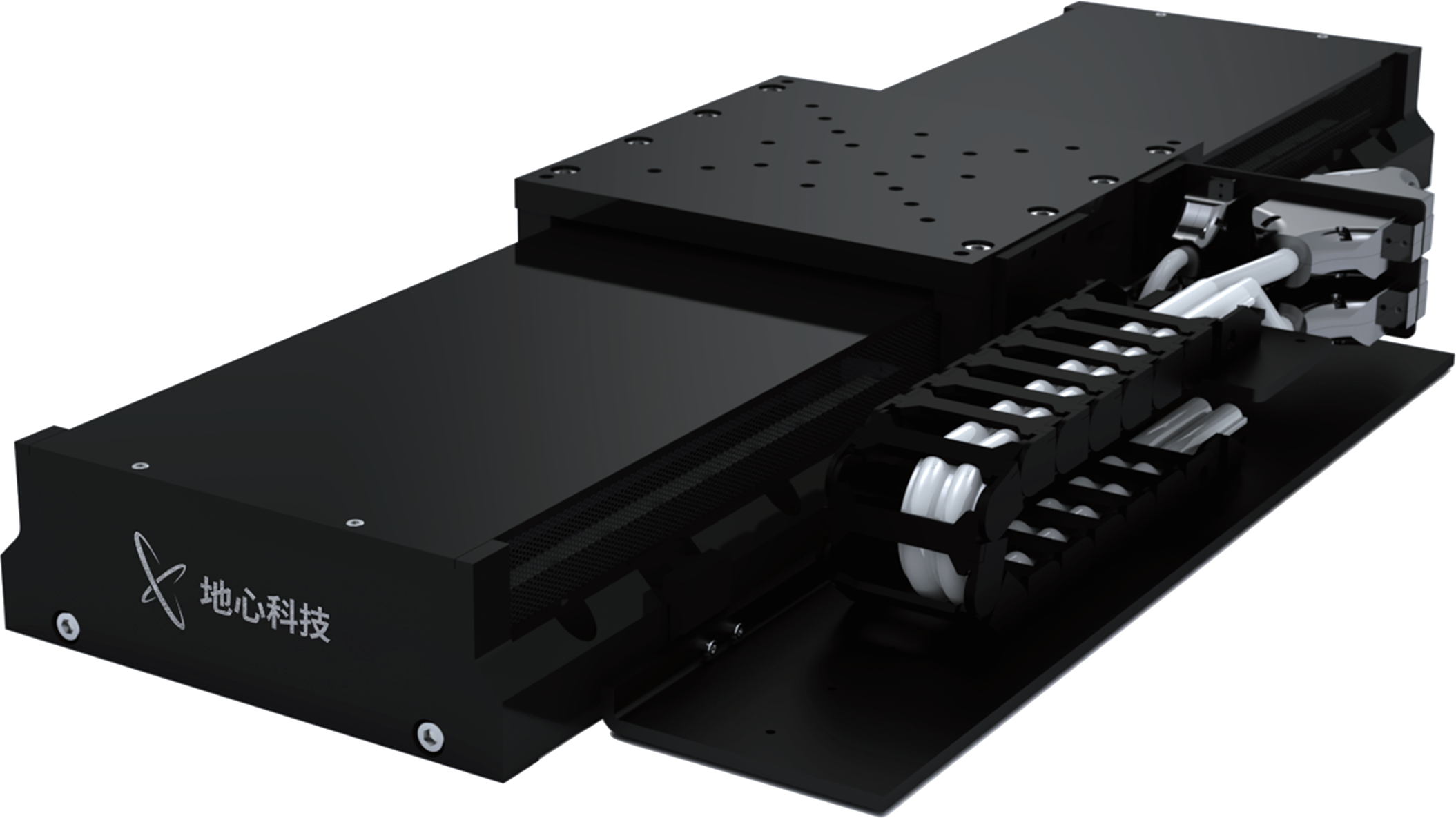
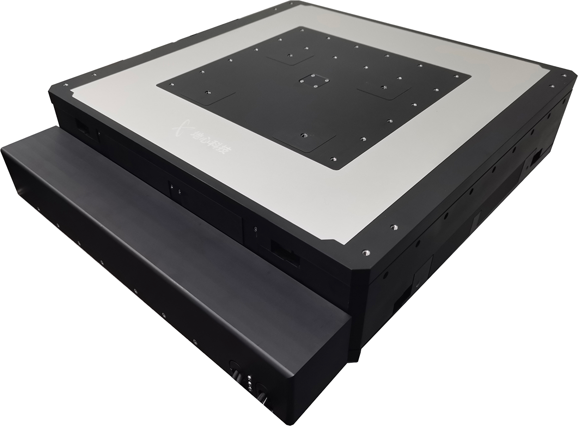
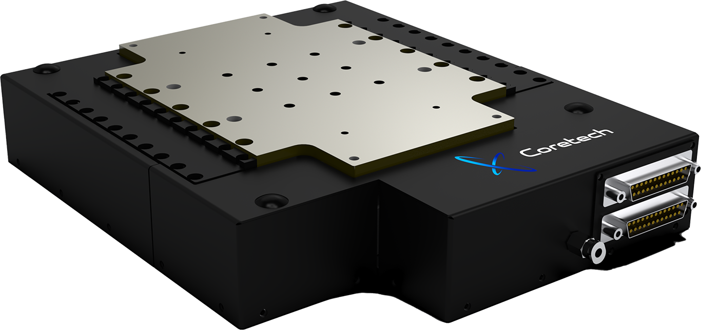
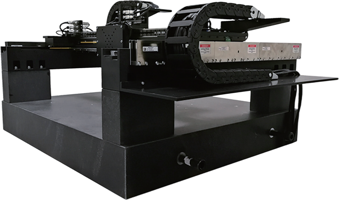
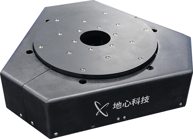
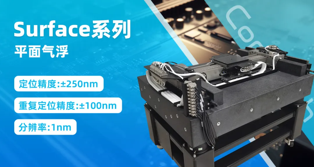
Surface Series Planar Air Bearing Stage
Delivers high-precision, high-speed positioning of chips/wafers while meeting the high cleanliness requirements of hybrid bonding.
High dynamic performance (cut-off frequency >330 Hz).
H-type structure with air guideways on both dual-drive axes and the beam axis.
Equipped with high-precision zero-coefficient-of-thermal-expansion grating feedback, featuring low expansion coefficient and minimal thermal drift susceptibility.
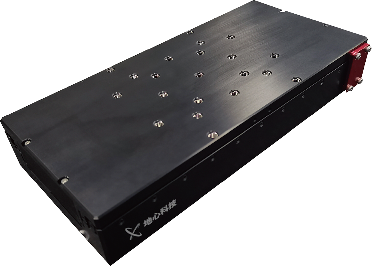
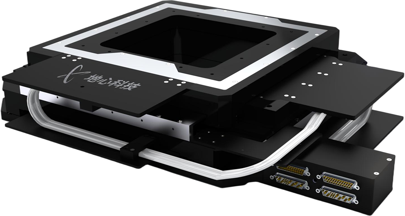
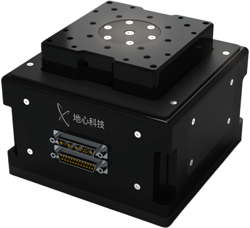
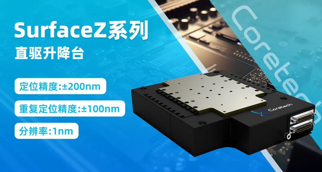
SurfaceZ Series Direct-Drive Z-Lift Stage
Precisely controls the upper-and-lower bonding process, ensuring smooth vertical motion to prevent chip/wafer damage.
High dynamic performance (no-load cut-off frequency >120 Hz).
Low lateral height, suitable for space-constrained applications.
In-position stability: 5 nm (configured with linear driver, in vibration-isolated laboratory environment).
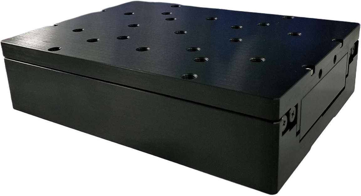
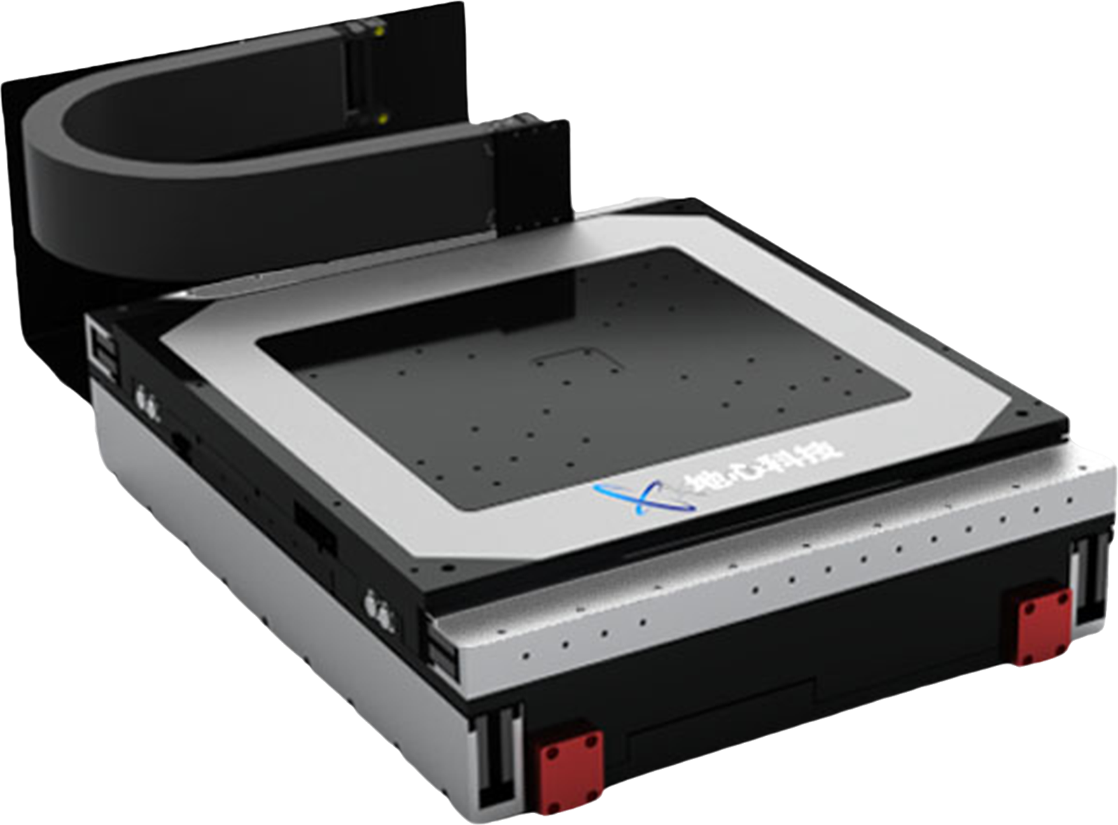
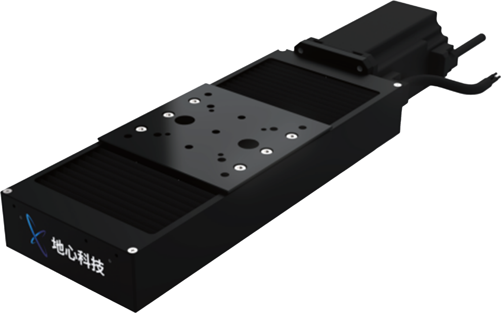
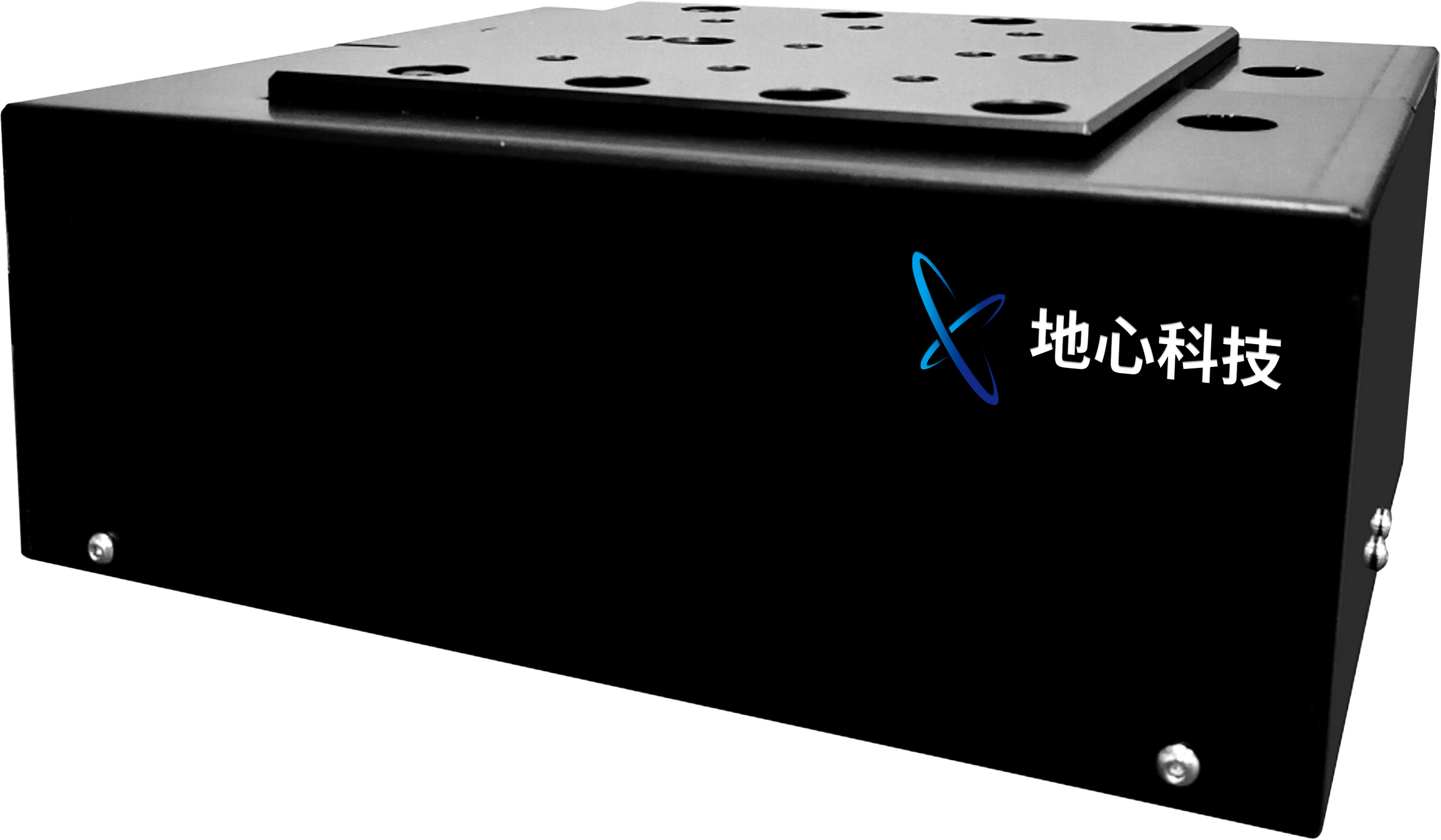
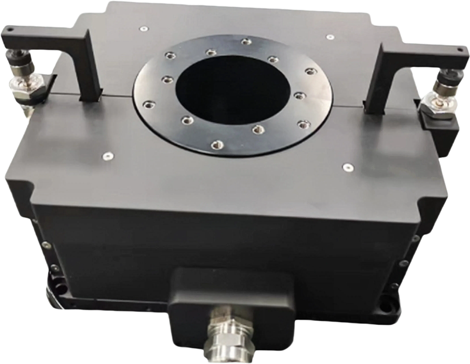
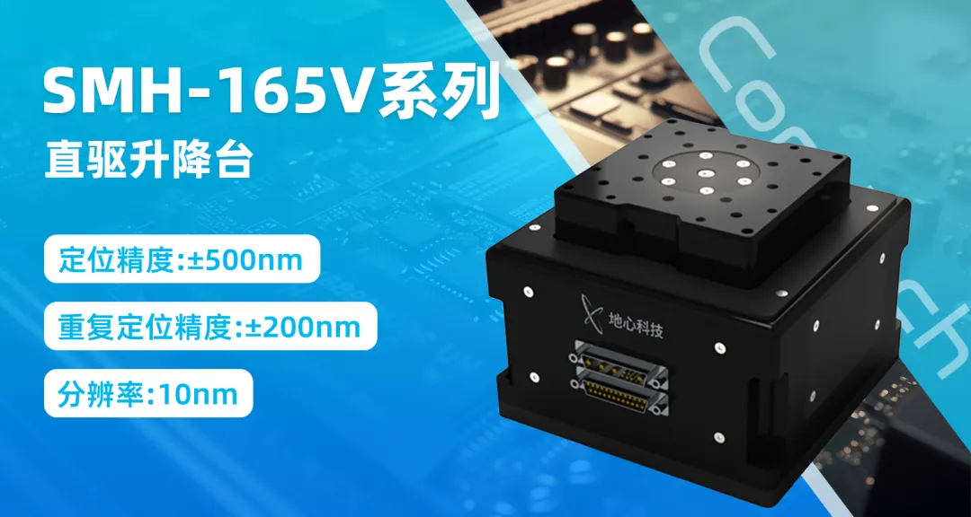
SMH-165V Series Direct-Drive Z-Lift Stage
Precisely controls the upper-and-lower bonding process, ensuring smooth vertical motion to prevent chip/wafer damage.
Flexible configuration with optional travel ranges and power-off self-locking functionality.
Minimum step: 20 nm; repeatability: ±200 nm; positioning accuracy: ±500 nm.
In-position stability: 20 nm (configured with linear driver, in vibration-isolated laboratory environment).
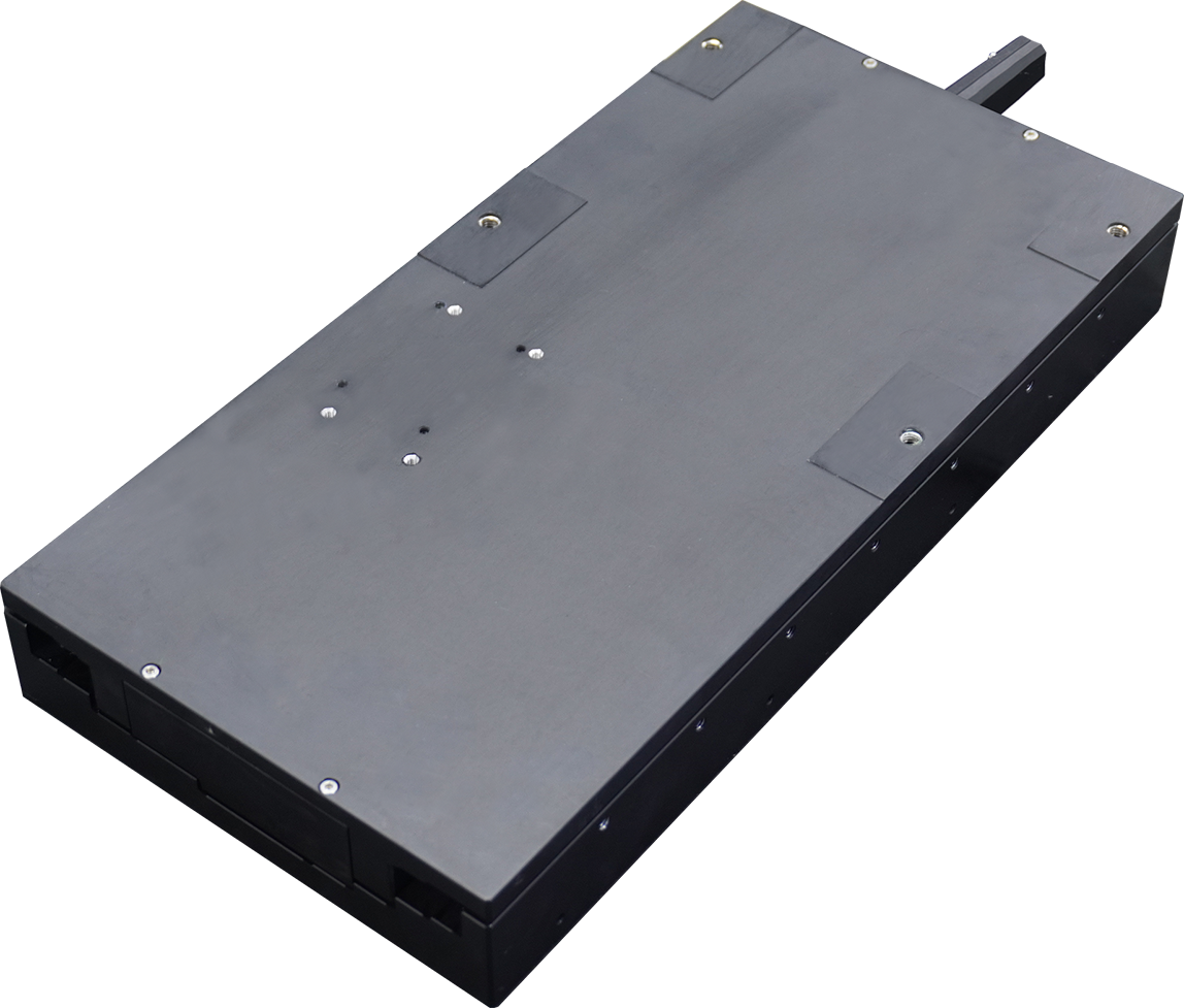
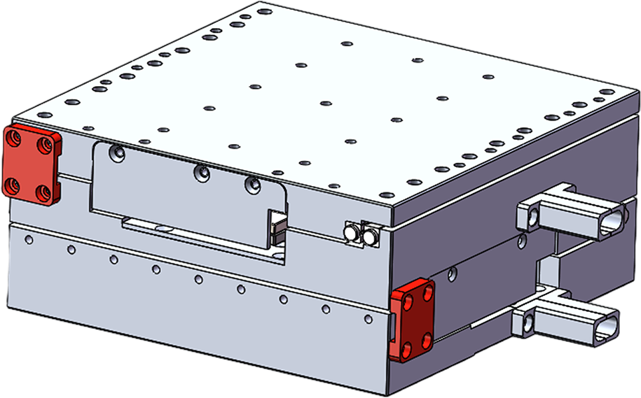
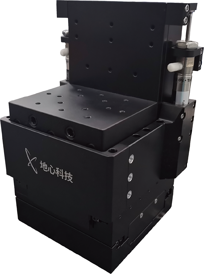
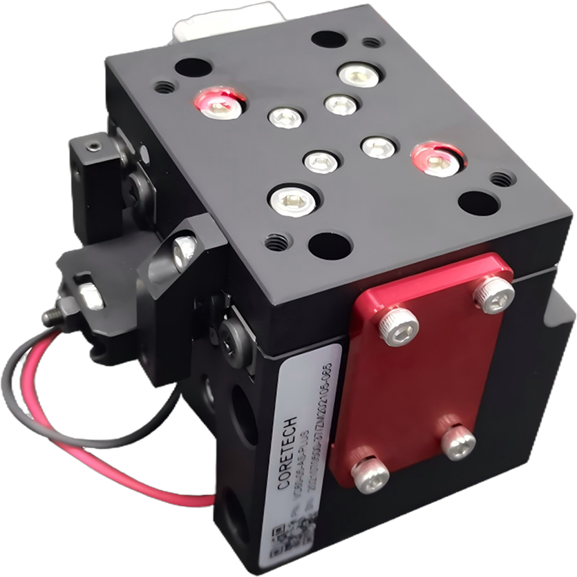
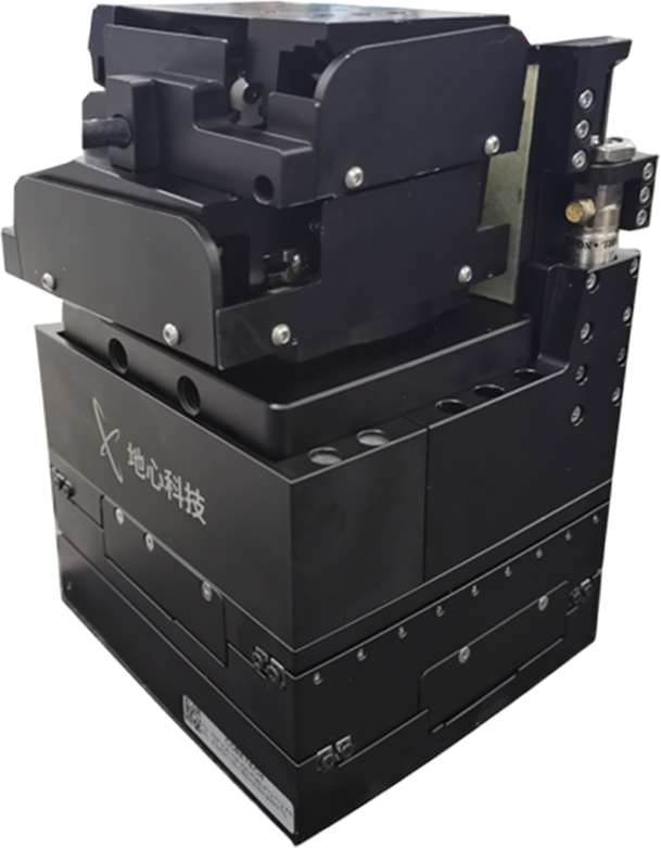
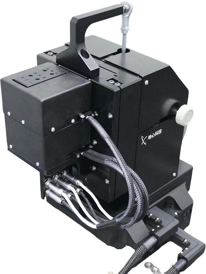
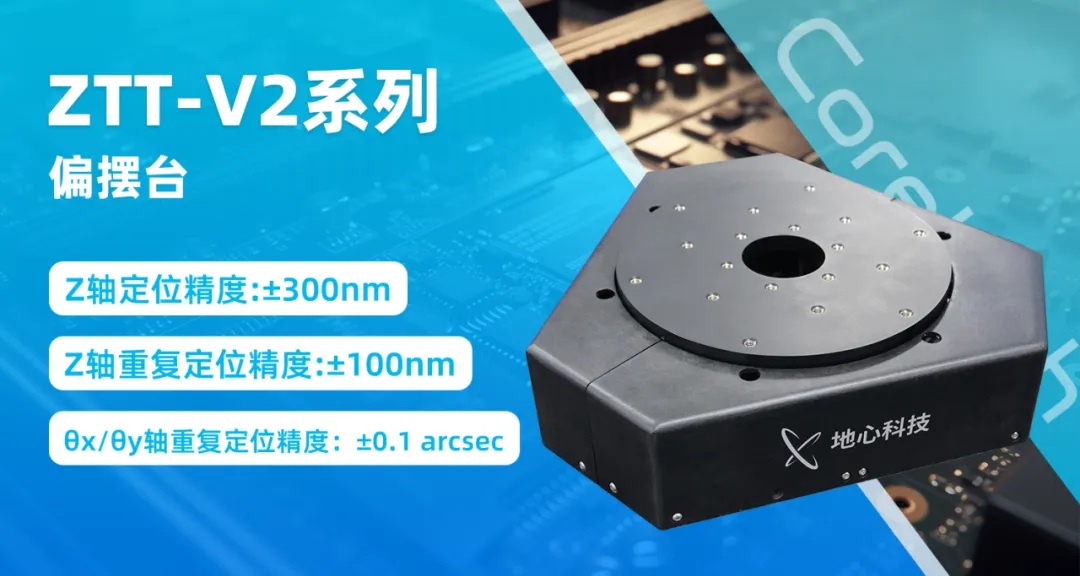
ZTT-V2 Series 3-Axis Tip-Tilt-Z Stage
Real-time adjustment of chip/wafer height and posture to ensure uniform contact across the entire bonding interface, preventing local non-bonding or stress concentration.
Integrated Z-lift and tip-tilt levelling platform.
Spherical hinge structure enabling multi-axis coordinated control.
Z-axis micro-step: 20 nm; Tip-tilt micro-step: 0.05 arc sec.
Beyond standard products, Geocentric Technology offers in-depth customisation across critical dimensions such as accuracy, number of axes, and travel based on specific customer requirements, delivering tailored motion platform solutions to facilitate efficient project implementation.
From the grand architecture of heterogeneous integration to the minute interconnections of hybrid bonding, every major leap in advanced packaging technology relies on solid support from underlying motion control precision. Building upon this foundation, Geocentric Technology will continue to provide state-of-the-art high-precision motion stages, empowering customers to achieve generational leaps in integration density, system performance, and production yield, and to secure a competitive edge in the next phase of the semiconductor industry.
Featured News
From Optical Chip Manufacturing to Fiber Coupling: Ultra‑Precision Motion Control Platforms Enabling a Technological Leap in the Optical Communications Industry
2026.06.03
ASP Series Ultra‑High‑Speed, High‑Precision Air‑Bearing Rotary Stage – Maximum Speed 5000 RPM
2026.06.03
In Micro/Nano Direct-Write Lithography Systems, the Stage's Exceptional Dynamic Performance Enhances Lithography Accuracy and Efficiency
2026.06.03
 Back to List