

.png)

.png)







Home
 News Center
Beyond Cost and Energy Advantages: How Precision Motion Stages Further Enhance Nanoimprint Lithography Accuracy
News Center
Beyond Cost and Energy Advantages: How Precision Motion Stages Further Enhance Nanoimprint Lithography Accuracy
News Center
Beyond Cost and Energy Advantages: How Precision Motion Stages Further Enhance Nanoimprint Lithography Accuracy
Beyond Cost and Energy Advantages: How Precision Motion Stages Further Enhance Nanoimprint Lithography Accuracy
 2026-06-02
Share:


Compared with EUV lithography, Nanoimprint Lithography (NIL) takes a different path. By leveraging the core principle of physical embossing combined with material curing, it significantly reduces process cost and energy consumption. However, NIL technology still faces considerable challenges in defect control during the manufacturing process, which limits its broader adoption. Precision motion stages may well be the key factor in breaking this deadlock.
01 Industry Background
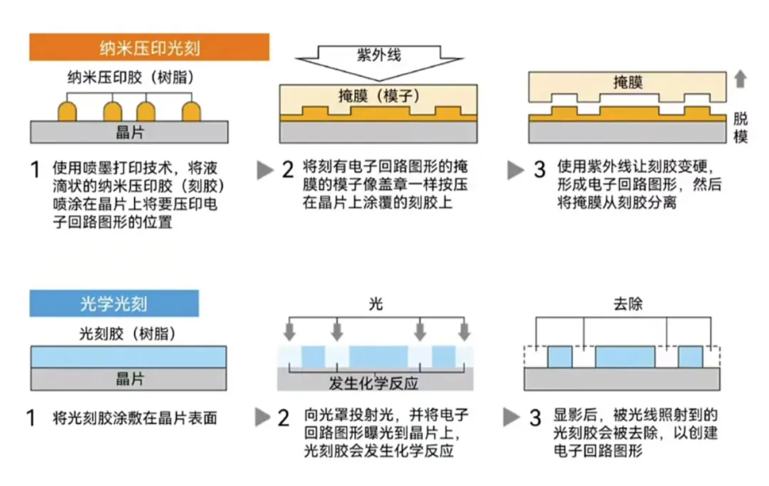
(Figure 1: NIL process flow, source: Canon official website)
Since the concept of nanoimprint lithography was first proposed by Professor Stephen Y. Chou in 1995, the technology has gradually transitioned from laboratory research to industrial production. On September 26, 2024, Canon shipped its most advanced nanoimprint lithography system, the FPA‑1200NZ2C, to the Texas Institute of Electronics (TIE), a semiconductor consortium headquartered in Texas, USA. The system enables patterning with a minimum linewidth of 14 nm and supports 5 nm‑node logic semiconductor production. In August of this year, Pulin Technology also launched its inkjet step‑and‑repeat nanoimprint equipment and delivered it to a domestic specialty process customer, marking an important milestone in China's high‑end semiconductor equipment manufacturing sector.
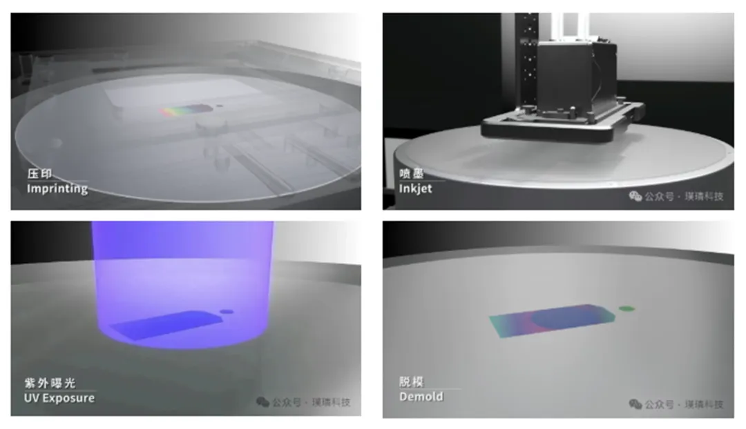
(Figure 2: Inkjet coating process flow, source: Pulin Technology)
The reason NIL technology has been able to break through ASML's monopoly in the EUV lithography space to a certain extent, and has gained market recognition, lies not only in its capability for 5 nm advanced nodes but also in the following outstanding advantages:
Significantly lower cost: According to Canon estimates, the cost of a four‑module J‑FIL nanoimprint system is only about one‑tenth that of an ASML EUV system. Additionally, NIL equipment is more compact, facilitating deployment in R&D and other scenarios. According to relevant data, the footprint of a cluster of four NIL systems is less than half that of an EUV lithography system, and the total equipment investment can be reduced to approximately 40% of an EUV production line.
Clear energy efficiency advantage: EUV lithography relies on high‑power CO₂ laser systems, with total power consumption reaching approximately 1 MW, whereas NIL equipment consumes only about 100 kW—a reduction of over 90%.
Despite its considerable potential, the difficulty of defect control during the production process remains the primary bottleneck constraining the large‑scale application of NIL technology.
02 Technical Challenges
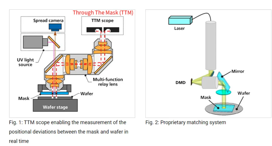
(Figure 3: Canon's conventional NIL overlay error measurement system)
The quality of the imprint template and defect control during the imprint process are the critical factors that determine whether NIL can achieve mass production.
The template is the foundation of nanoimprint lithography—any tiny defect on the template will be replicated across all wafers. The template itself demands extreme precision, and the heating/cooling or UV curing steps during the imprint process are inherently time‑consuming. Moreover, if the trajectory control during the demolding step is not precise enough, it can easily scratch the fragile and expensive template, significantly reducing its service life compared to non‑contact optical lithography masks, and thereby substantially increasing mass‑production costs.
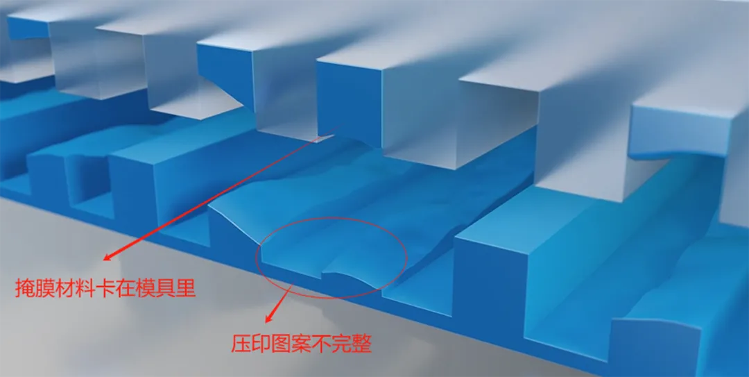
Insufficient overlay accuracy directly prevents yield improvement. Since NIL is a physical contact‑based imprint process, its overlay accuracy requirements are even more stringent than those of optical lithography. The industry has traditionally adopted a two‑stage "coarse + fine" positioning approach, but actual results remain unsatisfactory. The root cause lies in response delays and vibrations inherent in traditional cascade control, as well as minute mutual interference between multiple motion axes, which directly contributes to overlay errors and makes it difficult to achieve nanometer‑level stable alignment at high speeds. To address this issue, Canon's FPA‑1200NZ2C adopts a "step‑and‑repeat" operating mode: each step precisely aligns and imprints only one chip area (die), rather than aligning and imprinting the entire wafer at once. Aligning each die requires frequent start‑stop motions, demanding that the motion stage maintain nanometer‑level positioning accuracy while delivering high dynamic performance—presenting new challenges to the motion platform.
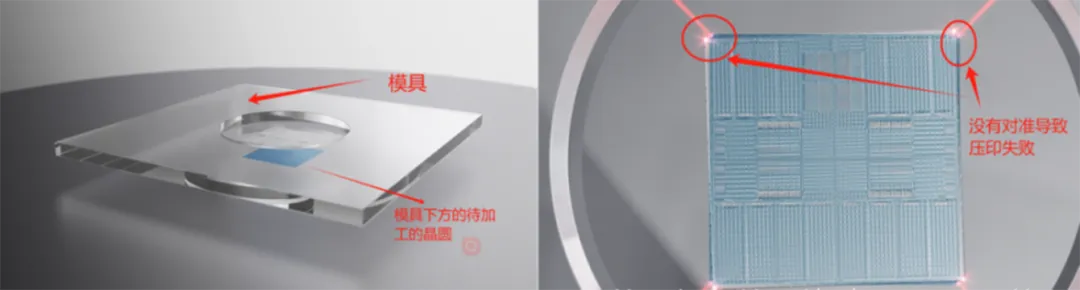
(Figure 5: NIL alignment, source: Yingci Fund)
03 Ground Motion Technology's Solution
As a core component of NIL technology, precision motion stages directly determine the quality and reliability of imprinted structures through their nanometer‑level motion accuracy. They play an indispensable role throughout the entire imprint process.
Ground Motion Technology has been deeply engaged in precision motion control for the semiconductor industry for many years, accumulating extensive practical application experience.
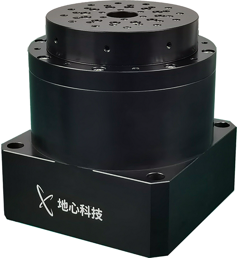
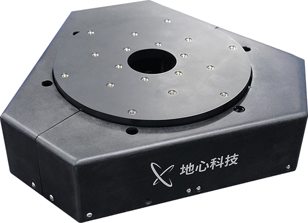
During the imprint process—whether for coating, substrate positioning, or imprint alignment and contact—multi‑axis precision motion stages achieve nanometer‑level accurate positioning, ensuring precise alignment with the template and improving pattern transfer accuracy.
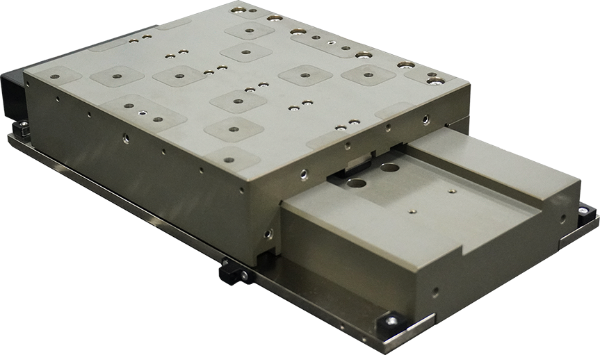
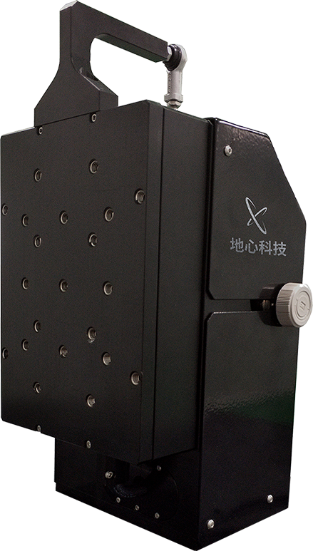
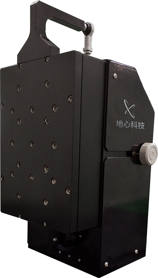
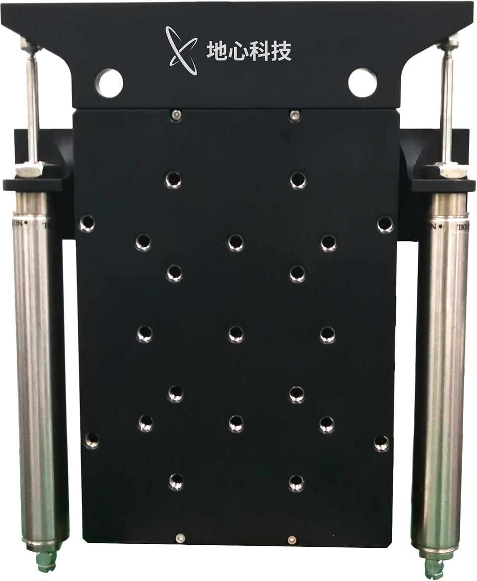
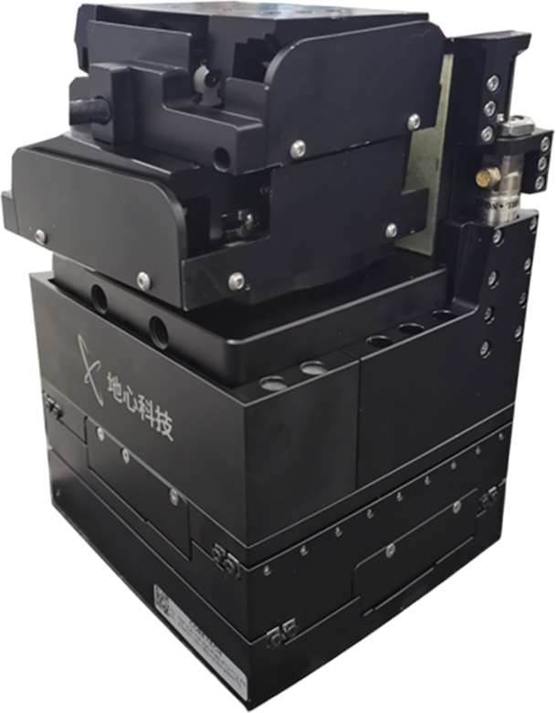
In pressure control and demolding, Ground Motion Technology's lift stages precisely control the imprint pressure and achieve smooth, accurate separation during demolding, effectively extending the template service life.
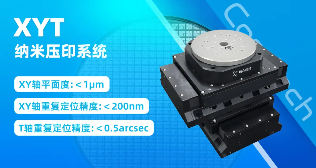
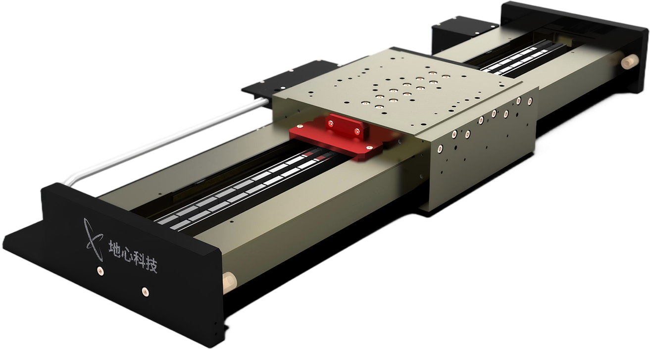
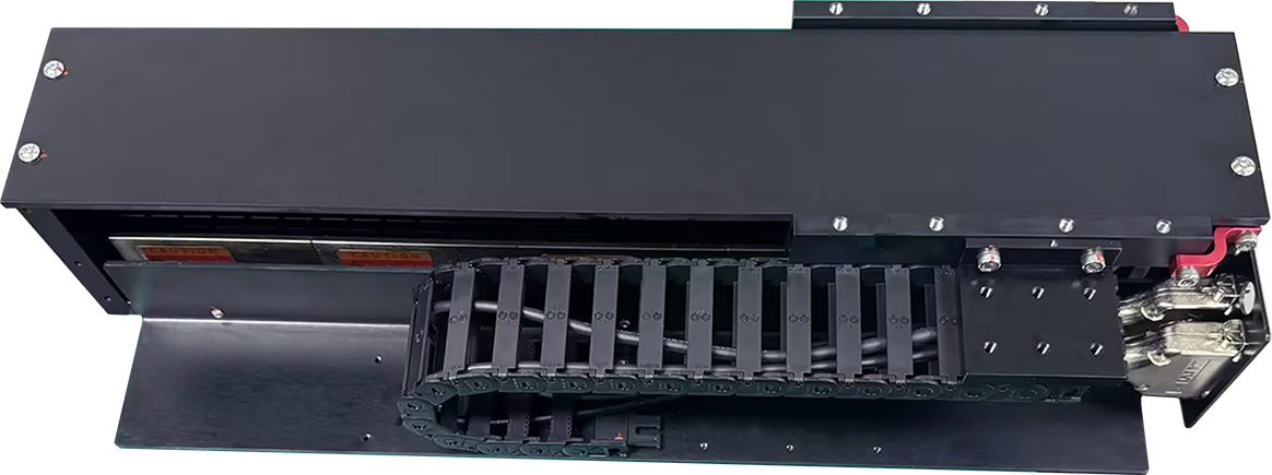
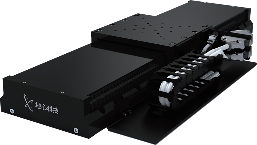
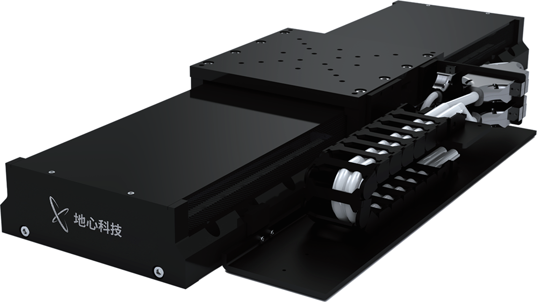
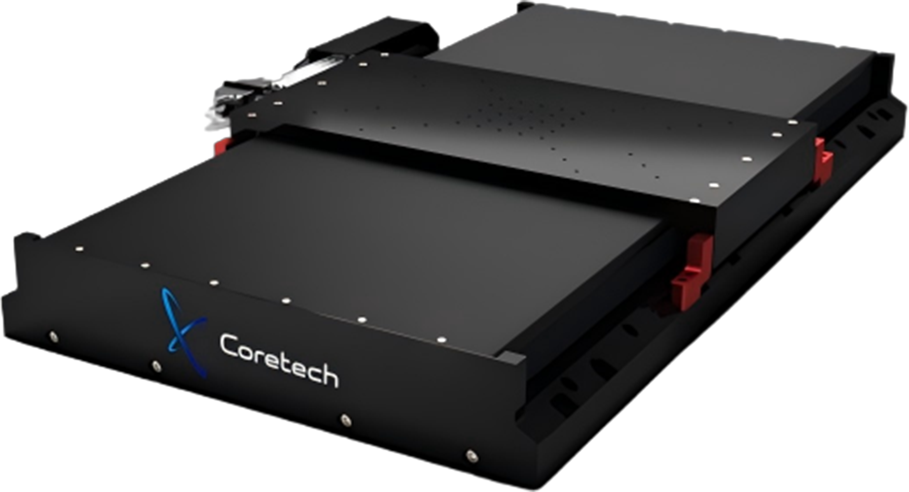
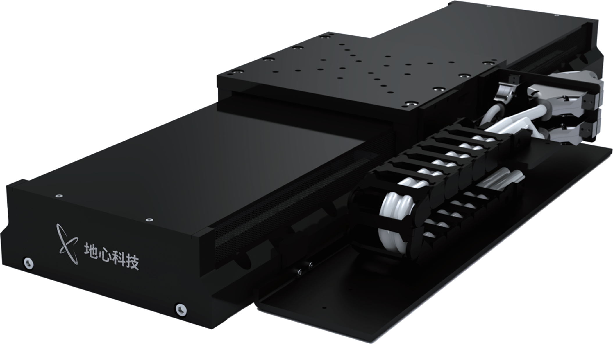
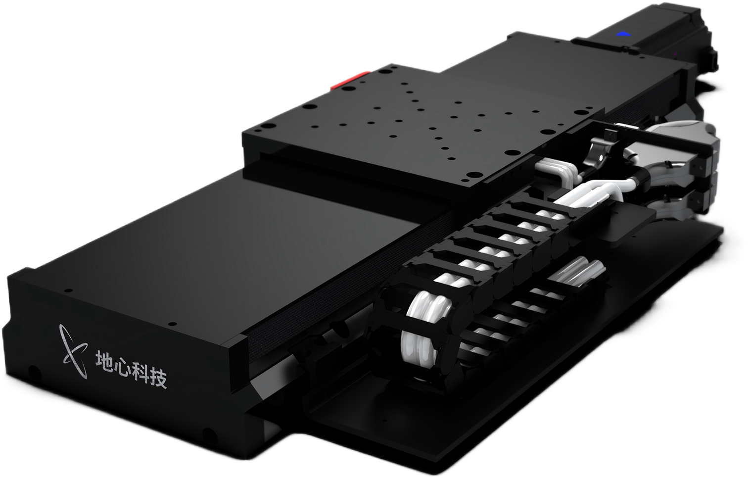
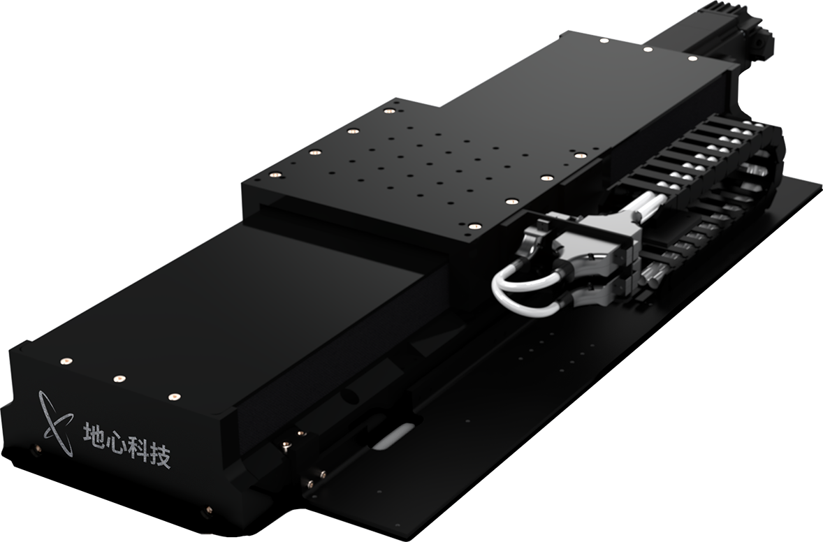
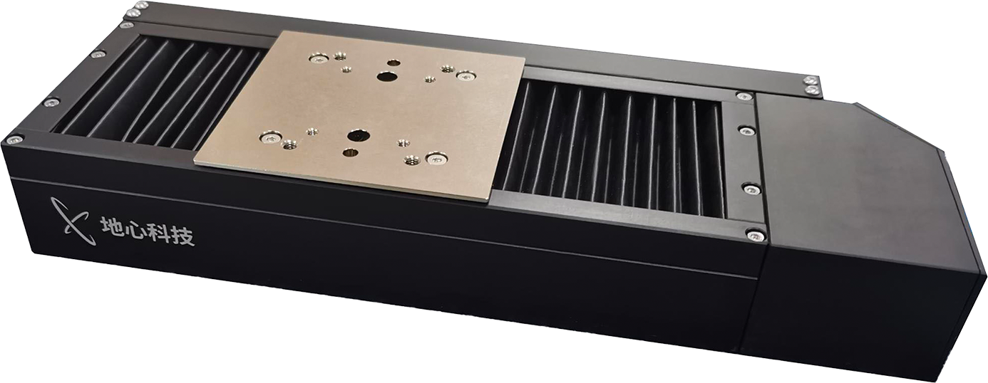
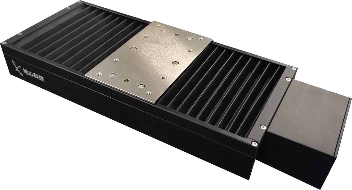
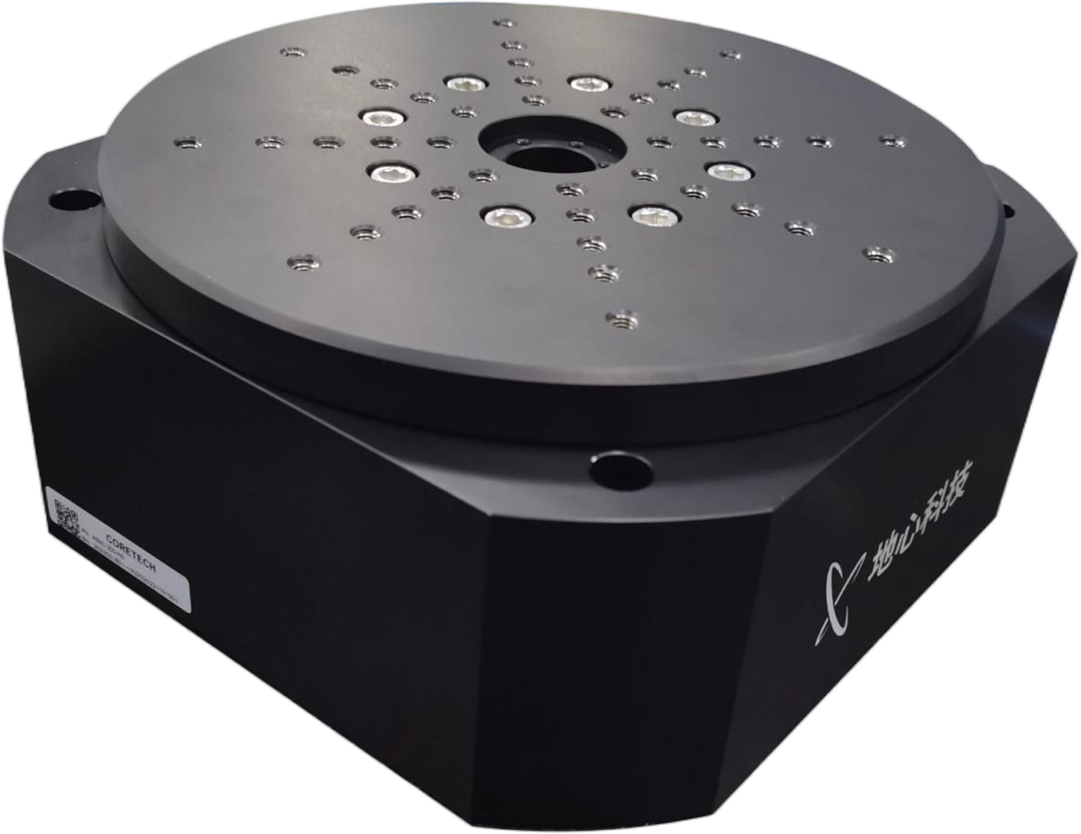
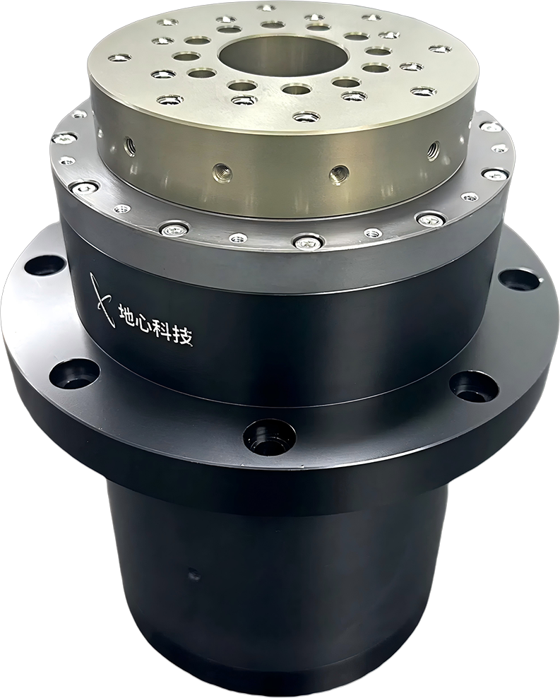
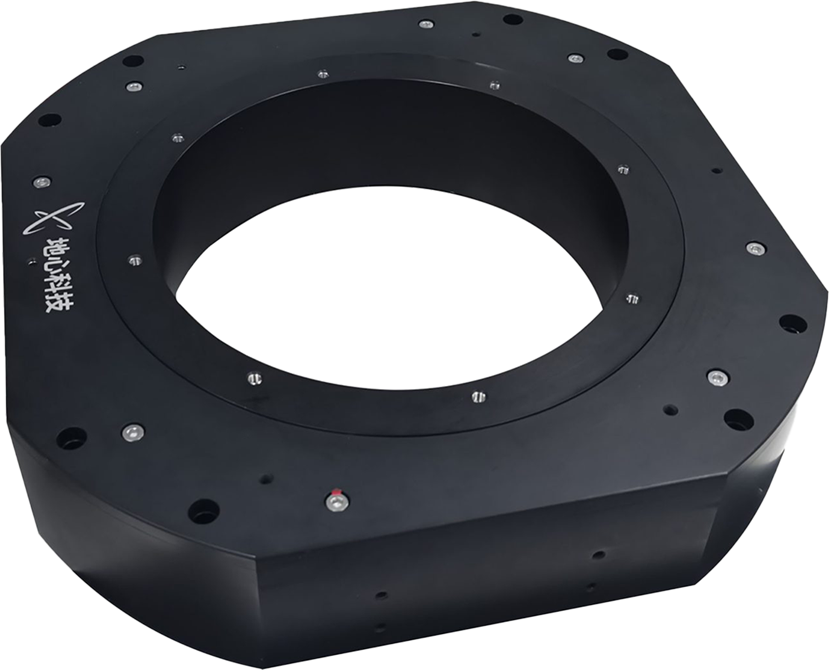
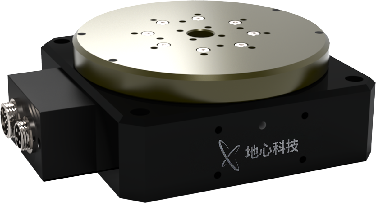
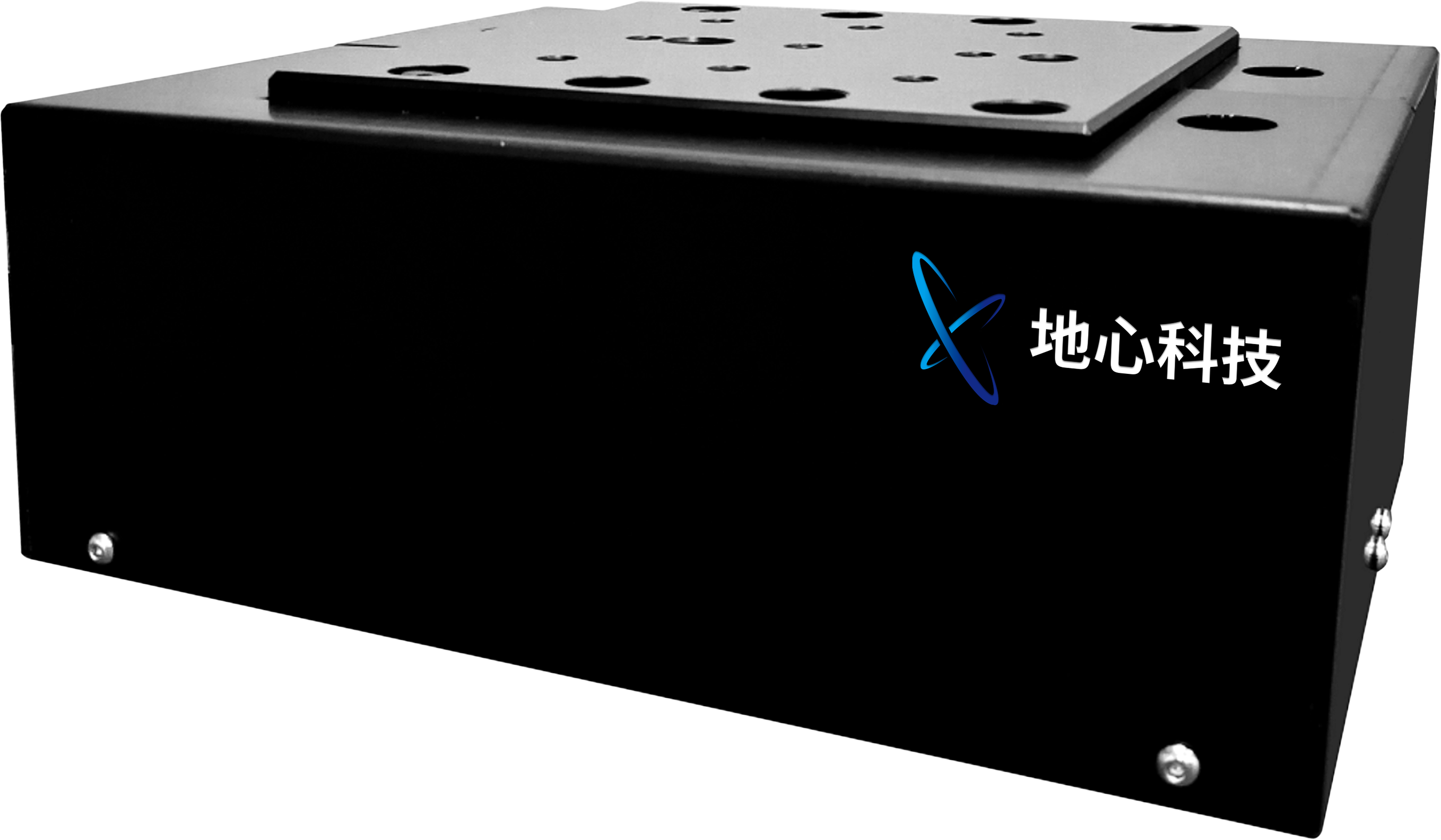
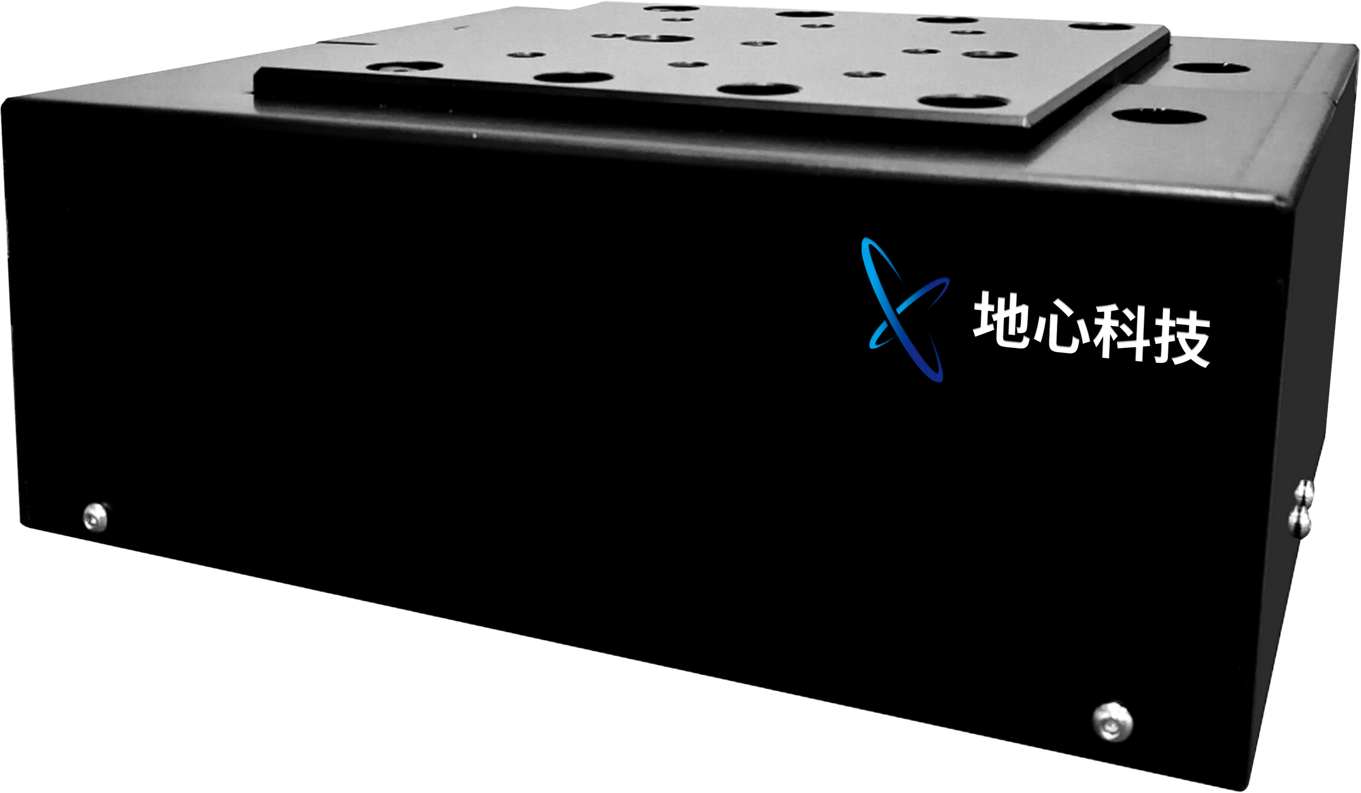
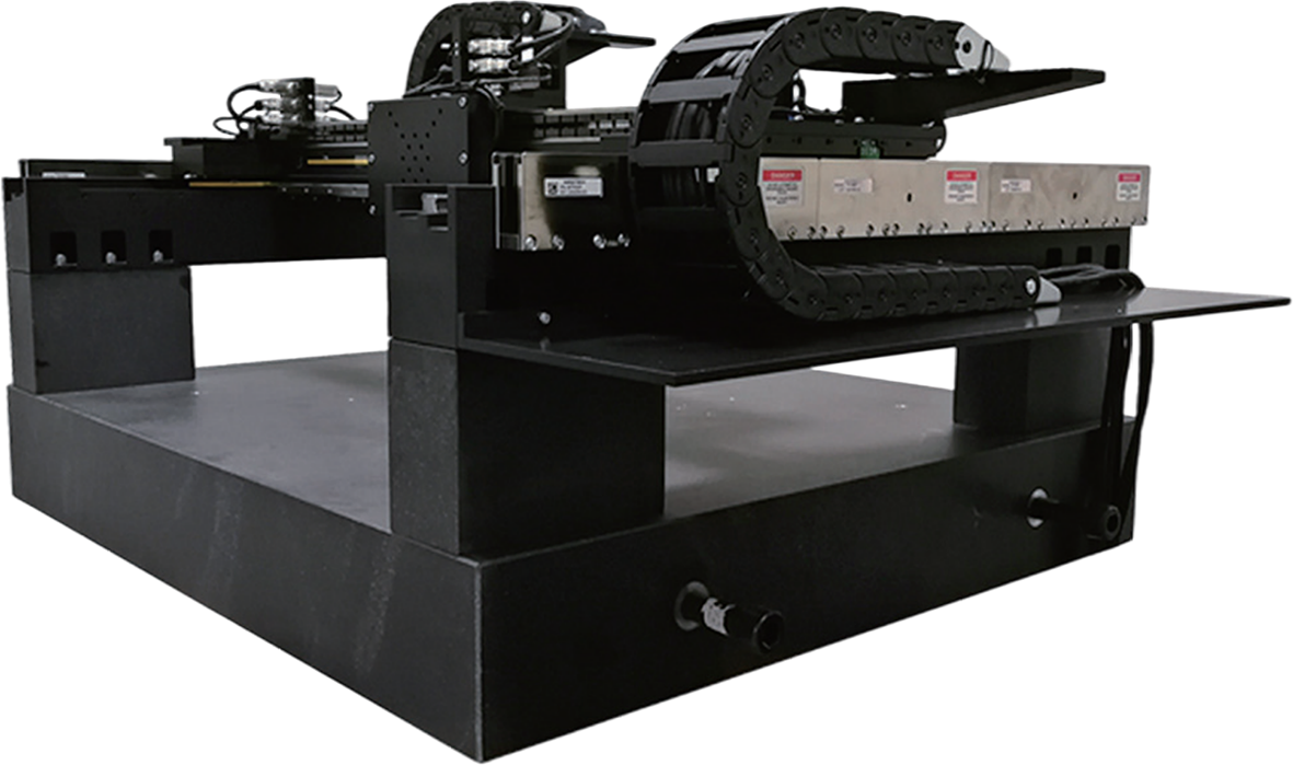
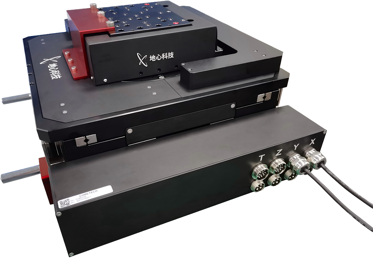
With the support of Ground Motion Technology, a leading company in micro‑ and nano‑manufacturing introduced a three‑axis (XYT) imprint system, significantly improving the overall performance of its NIL equipment and the quality of the final imprinted products. The X and Y axes of this system employ the SMH225LM series linear motor mechanical stages, with flatness better than 1 μm; they are equipped with the RSML series mechanical direct‑drive rotary stage. The X and Y axes achieve bidirectional repeatability positioning accuracy better than 0.2 μm, and the T‑axis accuracy is better than 0.5 arc‑seconds.
More Applicable Products
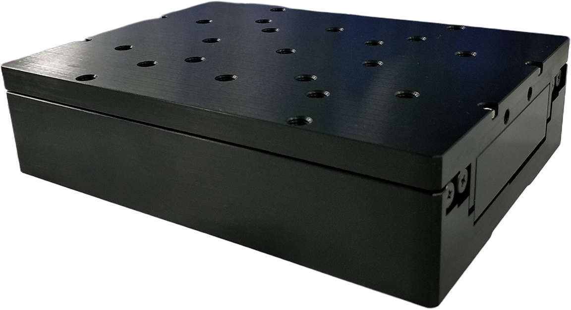
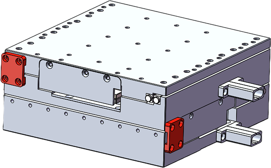
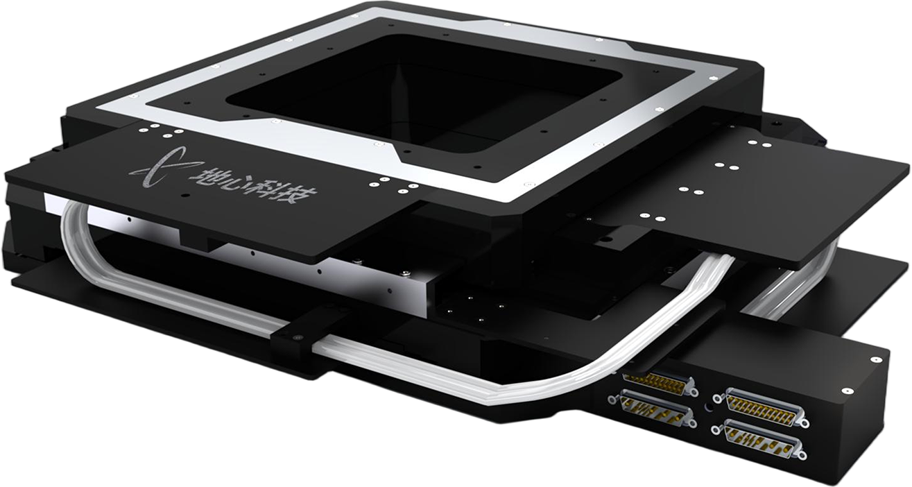
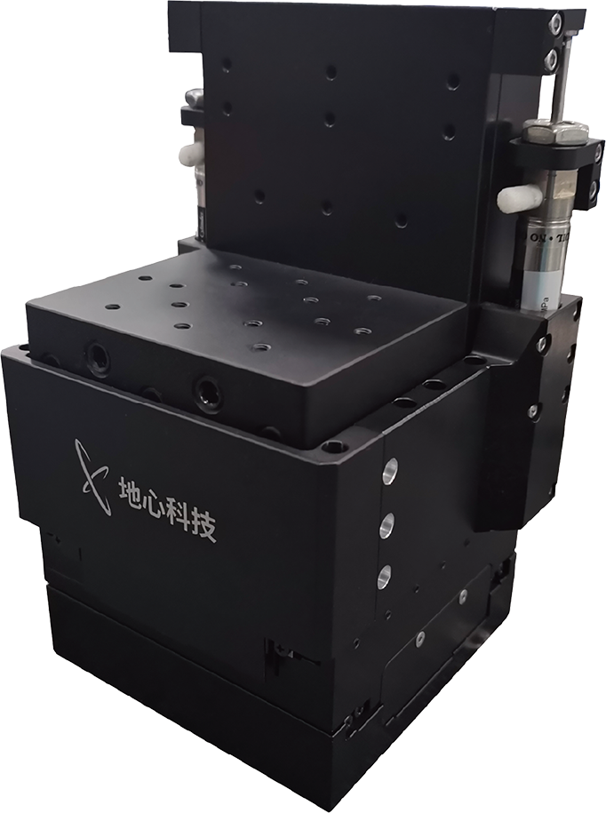
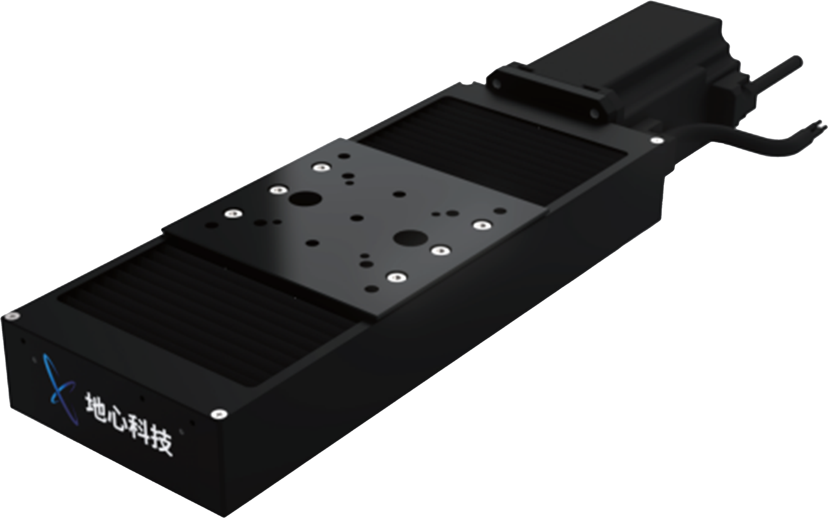
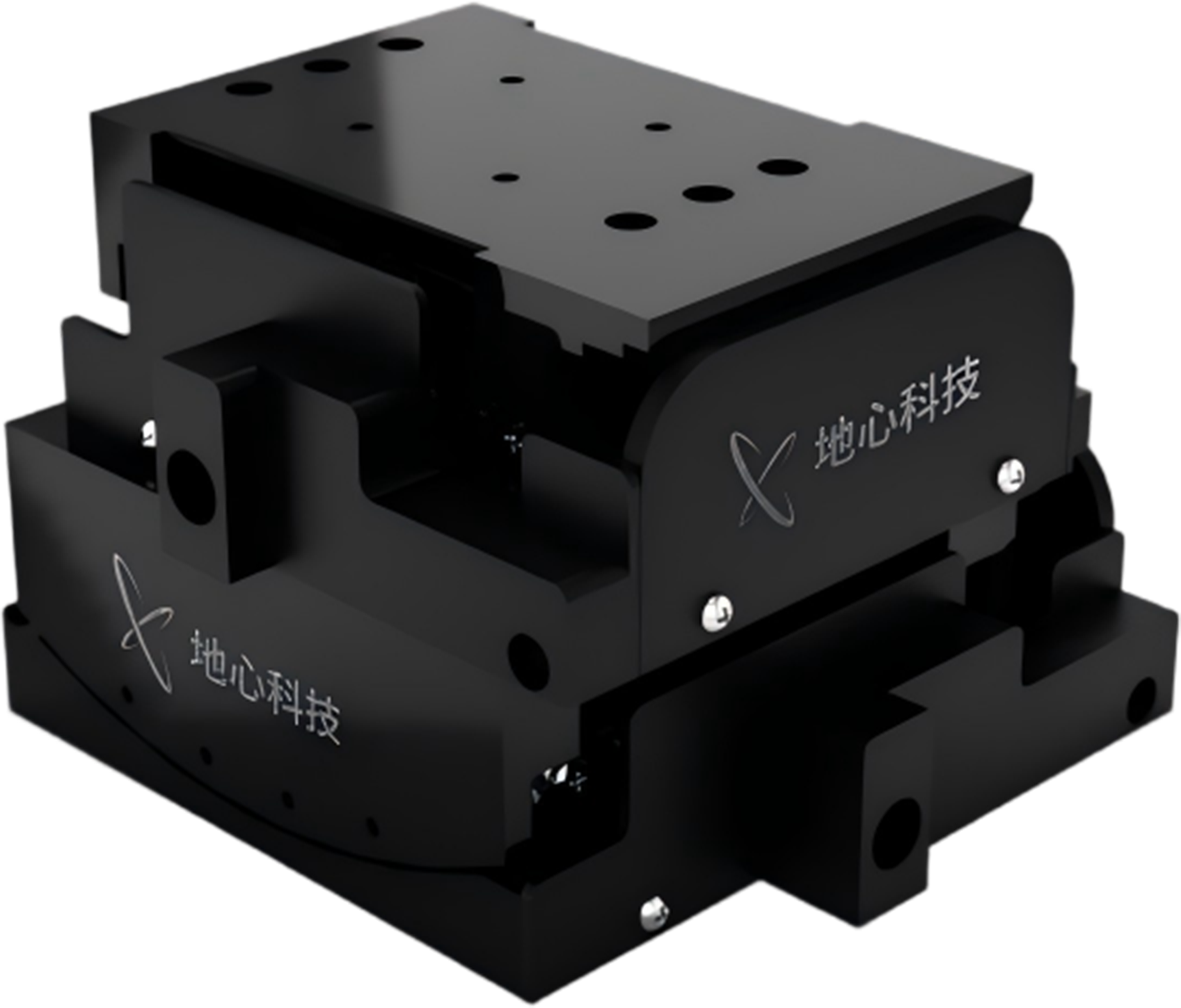
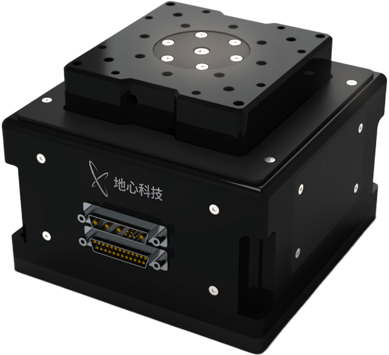
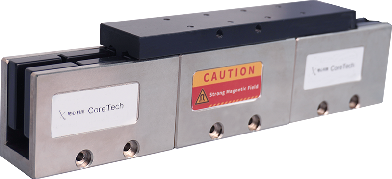
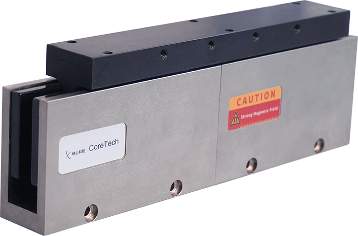
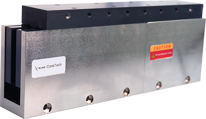
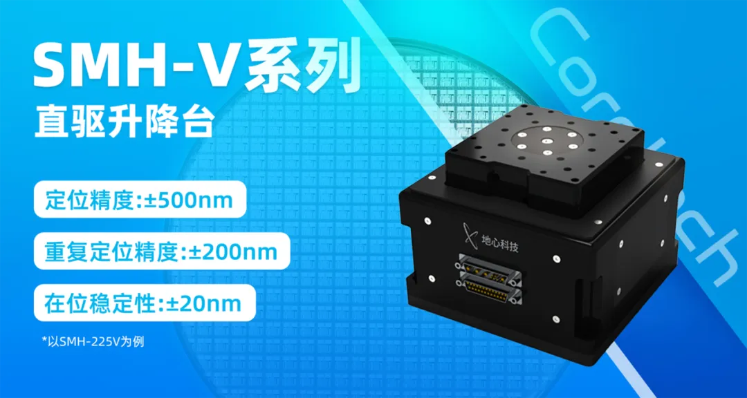
SMH‑V Series Direct‑Drive Lift Stage
Precisely controls the vertical contact process, accurately regulates imprint pressure, and enables smooth, accurate separation during demolding
Flexible configuration with optional strokes and power‑off self‑locking function
Minimum step: 20 nm; repeatability positioning accuracy: ±200 nm; positioning accuracy: ±500 nm
Resolution: 10 nm; in‑position stability: 20 nm (with linear drivers in a vibration‑isolated lab environment)
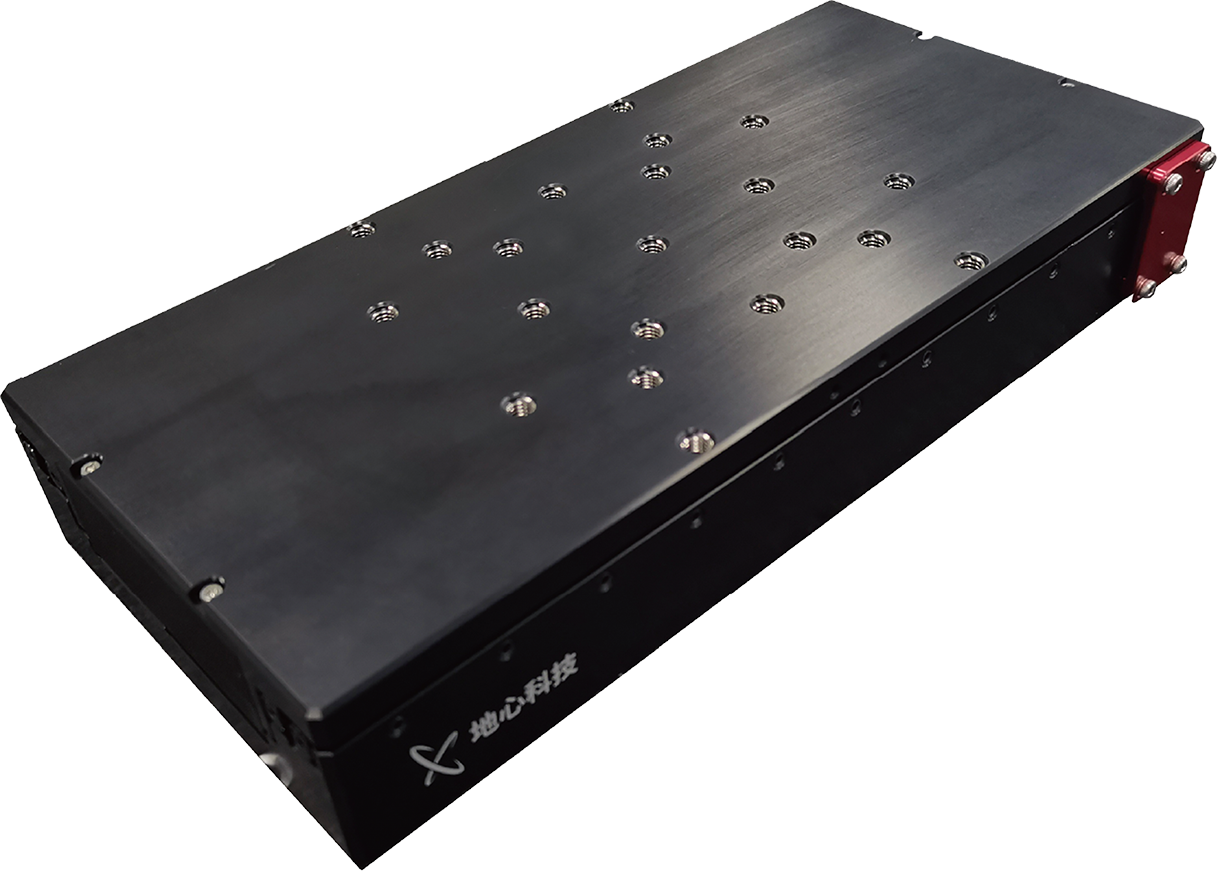
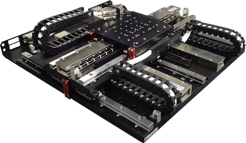
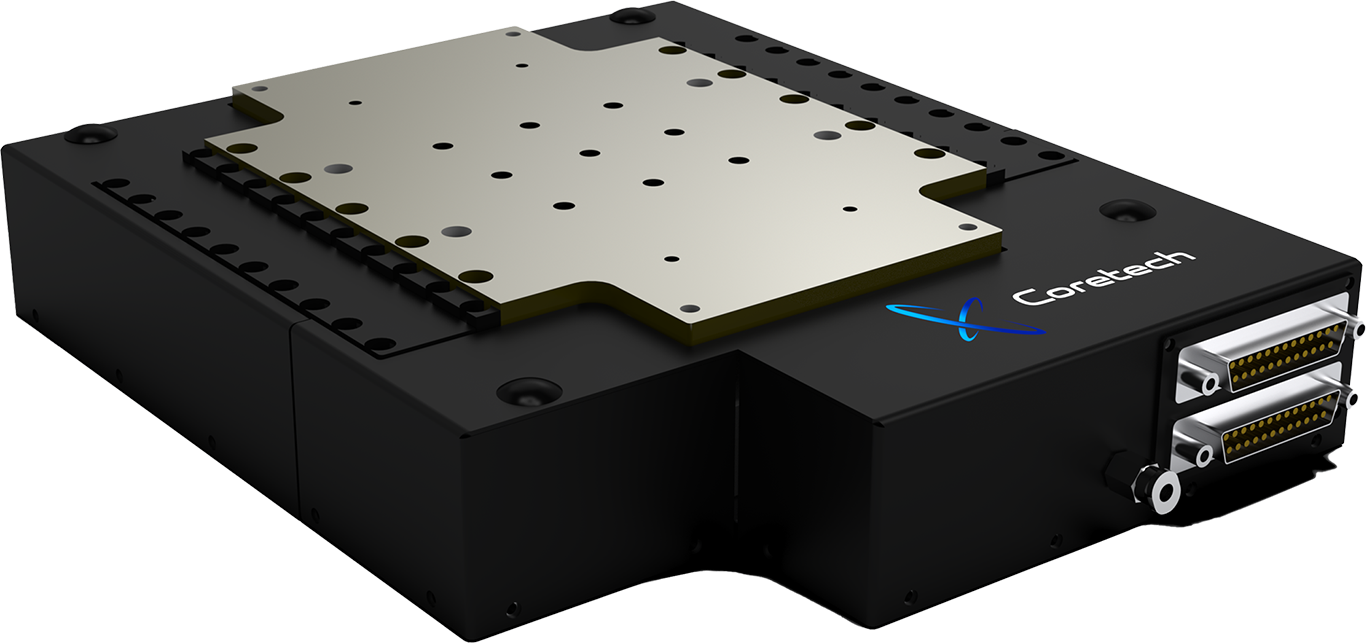
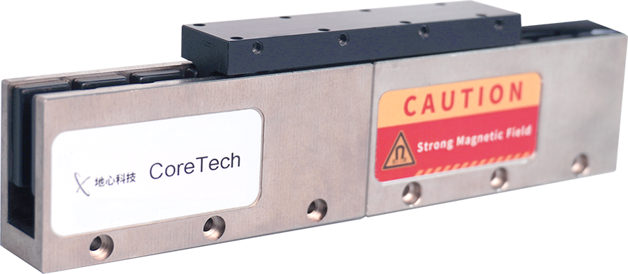
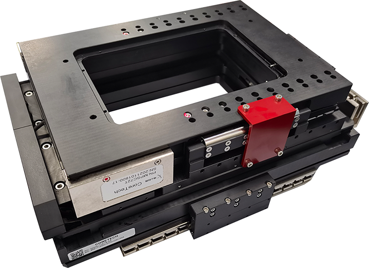
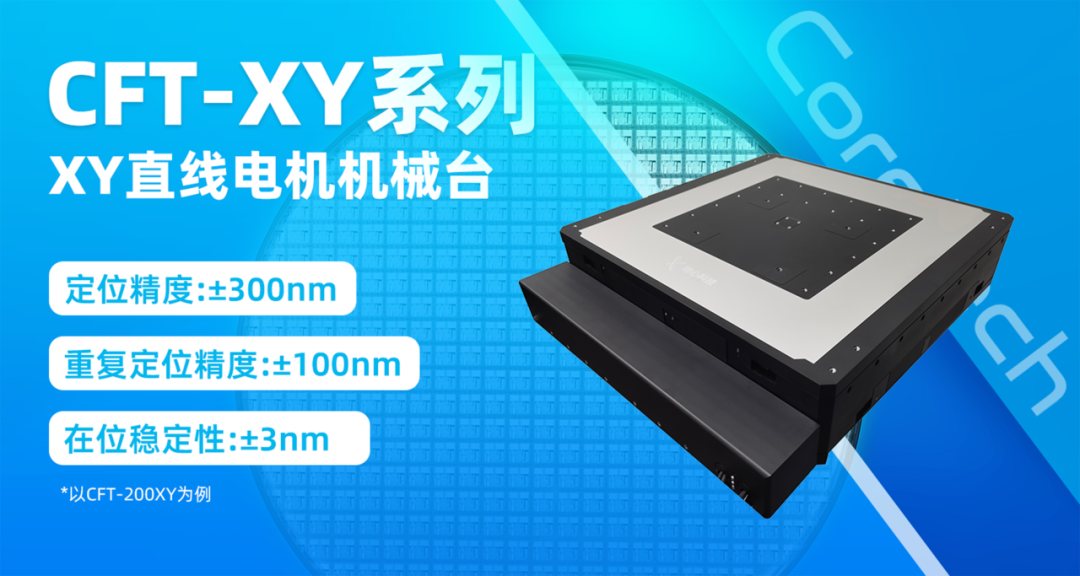
CFT‑XY Series XY Linear Motor Mechanical Stage
Achieves precise positioning for imprint alignment and contact, improving pattern transfer accuracy
Dual‑axis, four‑motor drive delivers excellent dynamic performance
Compact construction with low profile height and minimal Abbe error
Resolution: 1 nm; optional strokes of 200 mm × 200 mm and 300 mm × 300 mm
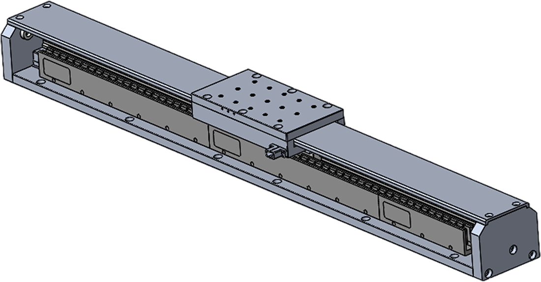
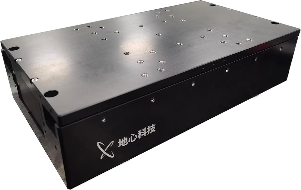
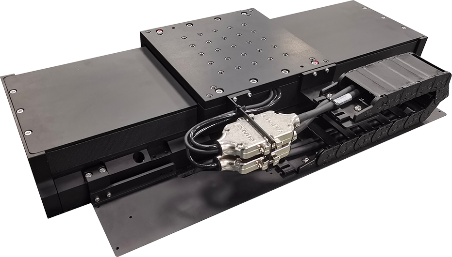
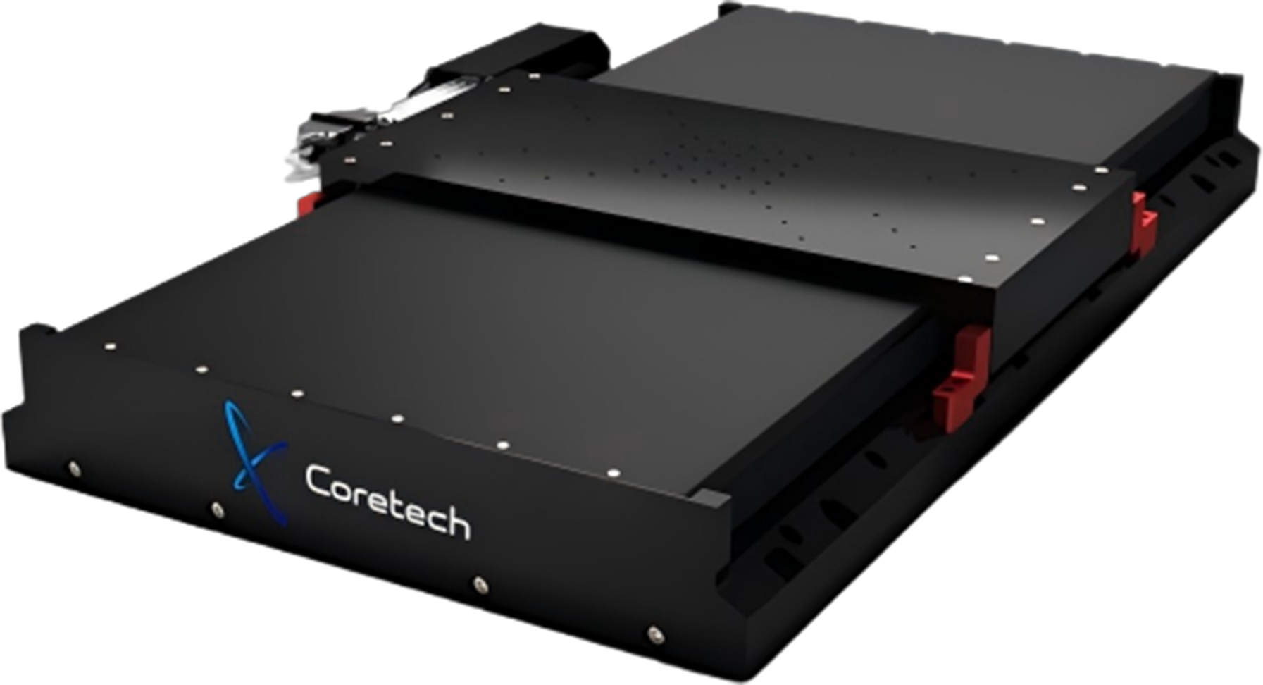
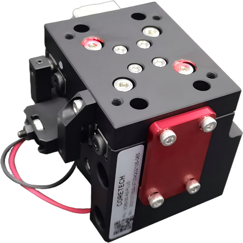
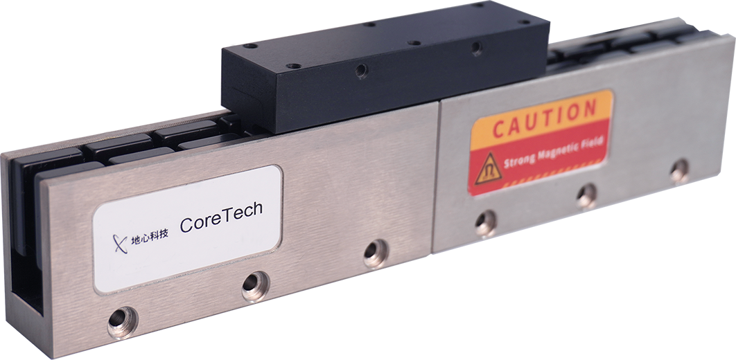
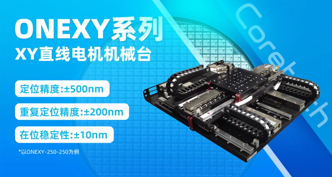
ONEXY Series XY Linear Motor Mechanical Stage
Achieves precise positioning for imprint alignment and contact, improving pattern transfer accuracy
Electronic resolution: 1 nm; minimum step < 20 nm
Rich stroke options combining large travel, high precision, heavy load capacity, and low profile height
Open architecture for easy integration into various multi‑axis configurations
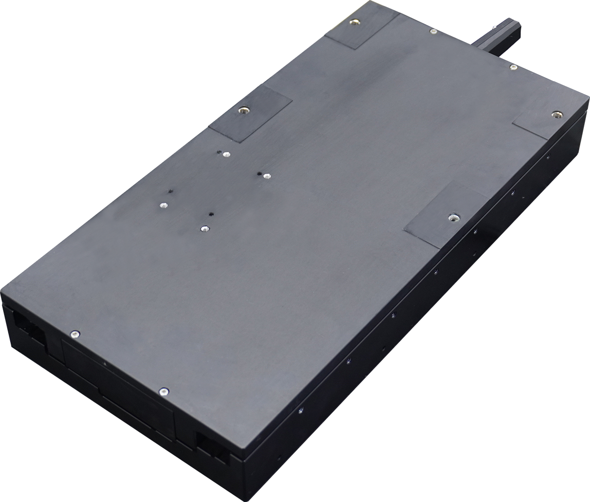
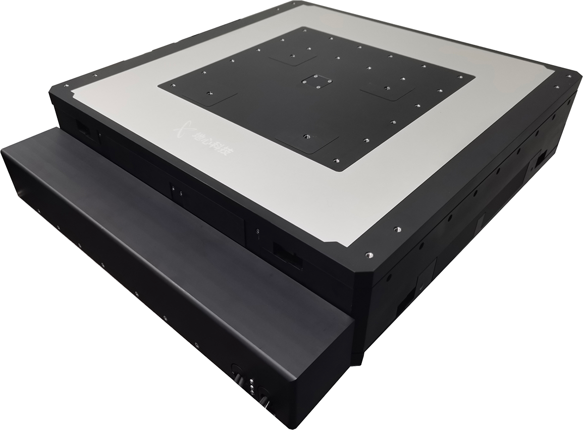
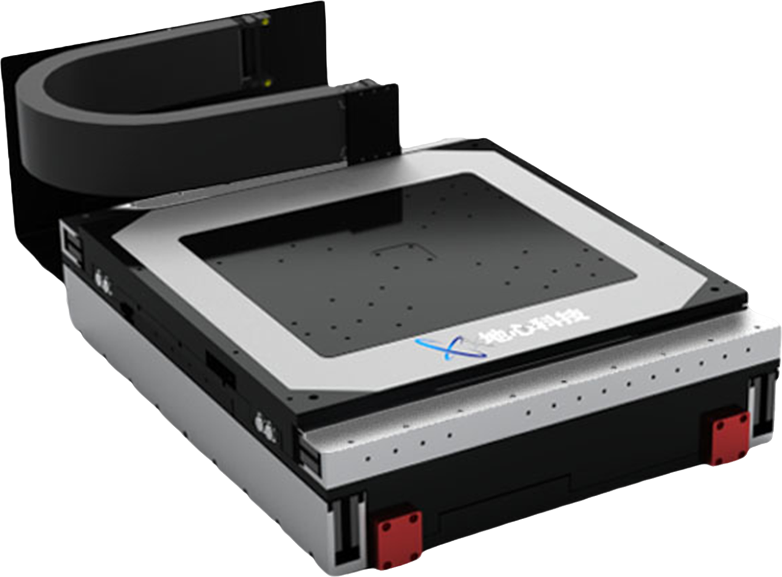
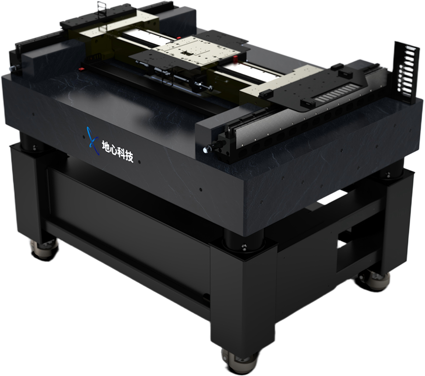
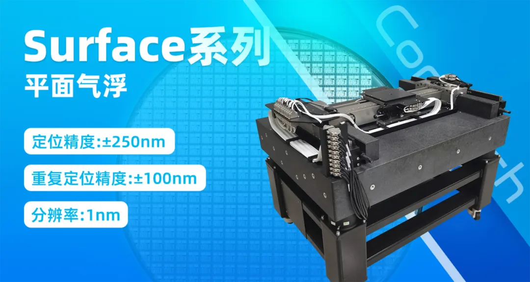
Surface Series Planar Air‑Bearing Stage
Achieves precise positioning for imprint alignment and contact, improving pattern transfer accuracy
High dynamic performance (cutoff frequency > 330 Hz)
H‑frame structure with air‑bearing guides on both dual‑drive axes and the beam axis
High‑precision zero‑coefficient‑of‑thermal‑expansion grating feedback for minimal thermal drift
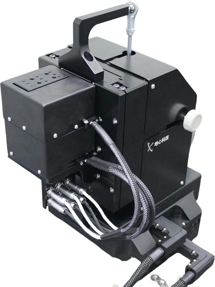
Beyond standard products, Ground Motion Technology also offers deep customization across key dimensions such as accuracy, axis count, and stroke, providing full life‑cycle precision motion control services to help customers efficiently realize their projects.
In response to the practical challenges NIL faces in defect control and template lifetime, Ground Motion Technology leverages high‑performance precision motion control as its core competency, providing critical support for NIL's transition to large‑scale mass production. Looking ahead, Ground Motion Technology will continue to deepen its technical expertise in nanometer‑level motion control and system integration. Together with industry partners, we aim to build more stable, more efficient, and more readily deployable nanoimprint motion control solutions, injecting new possibilities into global semiconductor manufacturing.
Featured News
Laser Processing Automation Solutions – 3D Spatial Drilling
2026.06.03
Laser Processing Automation Solutions – Wafer Grooving and LED Scribing
2026.06.03
Behind the Mass Production of Hybrid Bonding: How Precision Motion Stages Meet the High-Precision Control Demands of Semiconductor Packaging
2026.06.02
 Back to List