

.png)

.png)







Home
 News Center
A Comprehensive Overview of the HBM Manufacturing Process: What Role Does the High-Precision Motion Platform Play?
News Center
A Comprehensive Overview of the HBM Manufacturing Process: What Role Does the High-Precision Motion Platform Play?
News Center
A Comprehensive Overview of the HBM Manufacturing Process: What Role Does the High-Precision Motion Platform Play?
A Comprehensive Overview of the HBM Manufacturing Process: What Role Does the High-Precision Motion Platform Play?
 2026-06-03
Share:


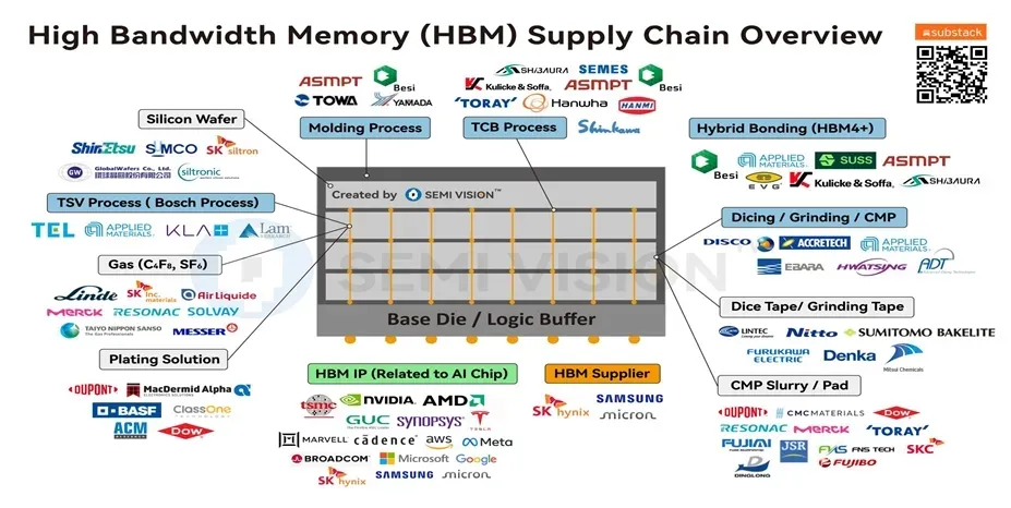
▲ Overview of the Global HBM Supply Chain (Image source: Ruixinwen)
HBM (High Bandwidth Memory) represents the highest-performance DRAM memory solution currently available. Its core technology involves vertically stacking multiple DRAM dies on a Logic Base Die through TSV (Through Silicon Via), and then achieving high-density interconnections via micro-bumps. The entire process falls within the realm of advanced 3D integration and is extremely challenging from a manufacturing standpoint.
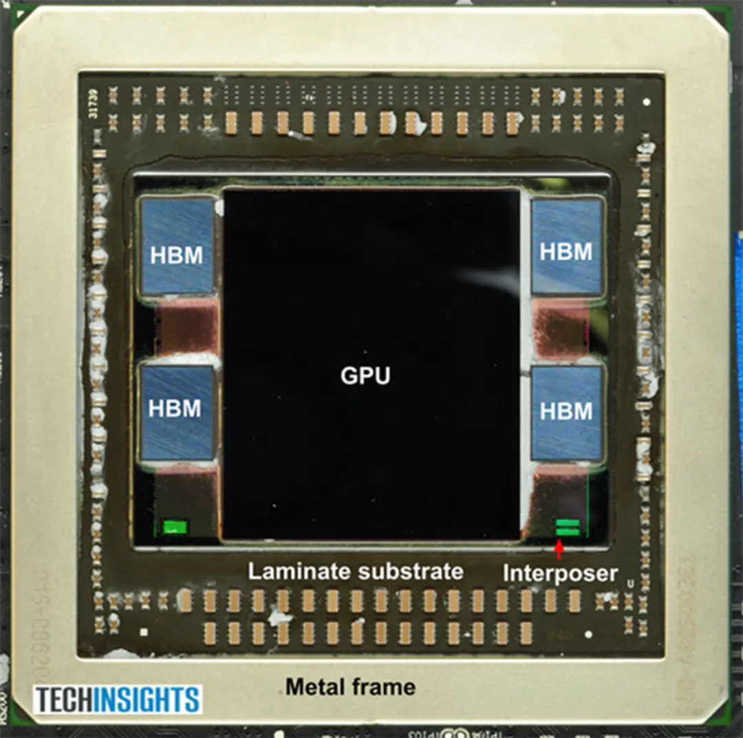
▲AMD Radeon 390X Fury X显卡,GPU裸片环绕四颗SK海力士HBM高带宽内存模块
In 2015, HBM made its first commercial deployment in an actual product—the AMD Radeon R9 Fury X graphics card—which utilized SK Hynix's first-generation HBM memory.
To this day, SK Hynix continues to hold the largest market share.
SK Hynix has already delivered samples of its next-generation 12-layer HBM4 to customers in March 2025, taking the lead in initiating mass production while simultaneously completing verification of 12-layer hybrid-bonded HBM. Samsung is mounting a strong recovery, with one of the key highlights of its HBM4 being the adoption of the more advanced 1c DRAM process node, achieving a speed of 11 Gb/s during Broadcom testing. Micron's HBM4 samples have also broken through the 11 Gb/s speed barrier, with bandwidth exceeding 2.8 TB/s, and are set to achieve the industry's first large-scale mass production shipment for the NVIDIA Vera Rubin platform in the first quarter of 2026.
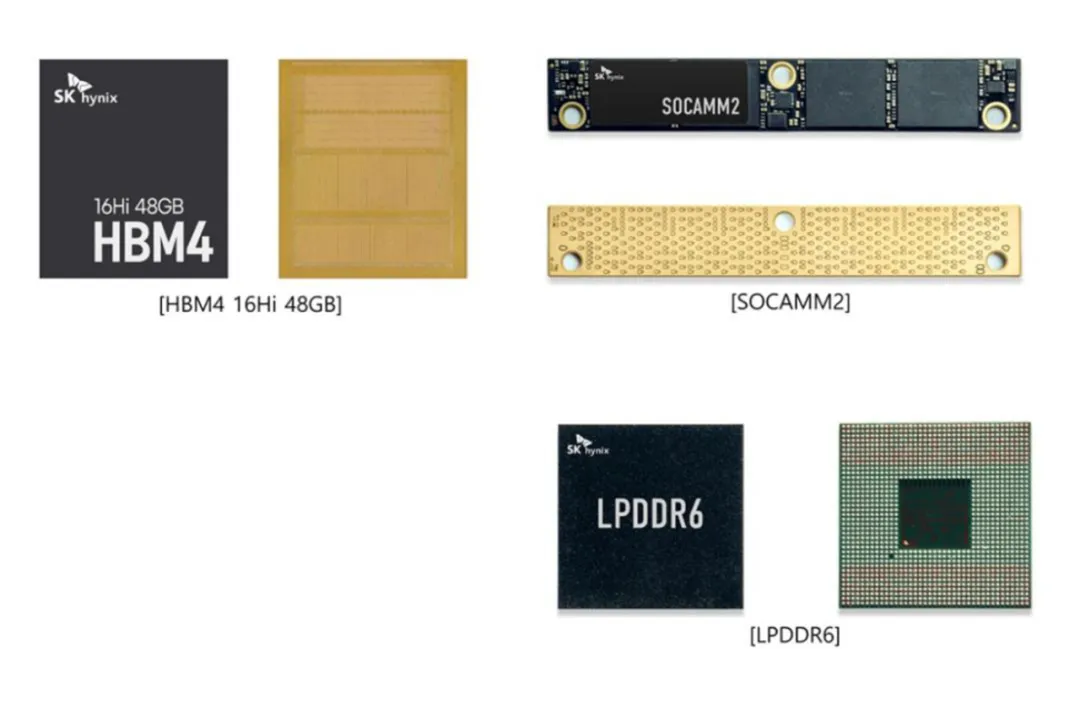
HBM is typically not manufactured as a standalone "processor"; rather, it is integrated with logic chips such as GPUs/AI accelerators/CPUs through 2.5D/3D advanced packaging to form high-bandwidth processor systems.
Throughout the entire manufacturing process, motion platforms are not merely auxiliary tools—they are a foundational enabling technology that facilitates HBM's evolution toward higher layer counts and greater bandwidth. Their precision levels directly define process boundaries and the feasibility of mass production. The higher the HBM generation, the more the process relies on motion control capabilities. In process steps such as lithography, die attach, bonding, and testing, errors at the micron or even nanometer scale can significantly impact HBM yield.
As bump pitch continues to shrink, integration density keeps increasing, and heterogeneous integration grows more complex, what specific role does the precision motion platform play in the HBM manufacturing workflow? And how does it support the stringent demands of next-generation advanced packaging processes?
·Key HBM Manufacturing Processes·
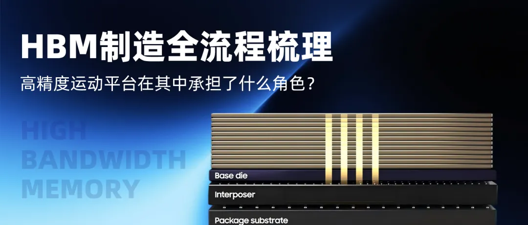
01 Front-End Process – Wafer Fabrication
This stage involves manufacturing high-performance DRAM chips and the Logic Die.
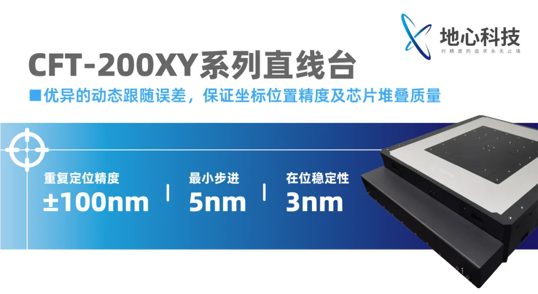
■ Lithography: The pinnacle of precision motion in semiconductor equipment, and the most critical step in the front-end process. Projection lithography remains the mainstream technology in semiconductor manufacturing, requiring motion platforms to maintain excellent in-position stability during high-speed motion, along with minimal step size and high repeatability positioning accuracy.
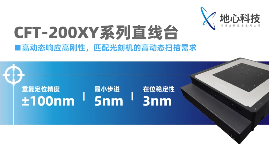
■ Etching and Ion Implantation: The wafer stage must possess extremely high repeatability positioning accuracy, providing a stable positional reference for high-precision ion implantation.
02 Mid-End Process – TSV and Bumping
This is the key step that distinguishes HBM from conventional DRAM, and also the stage where demand for high-precision motion platforms surges.
■ TSV Fabrication: Requires drilling tens of thousands of deep microscopic vias in the DRAM die and filling them with copper conductors. The TSV apertures are extremely small and demand very high verticality; both laser drilling and Deep Reactive Ion Etching (DRIE) require highly stable wafer stages.
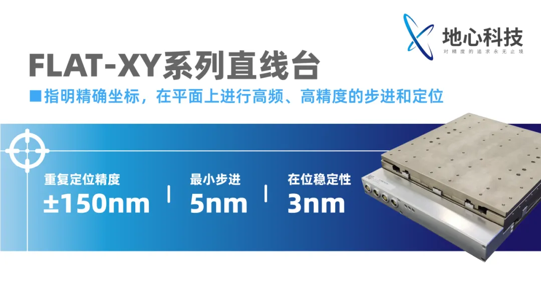
■ Bumping: The dimensions of micro-bumps (typically 5 μm × 5 μm) and their pitch (20 μm) are extremely small. Their positional accuracy directly affects the quality of subsequent die stacking, requiring precise positioning to ensure consistency across millions of bumps
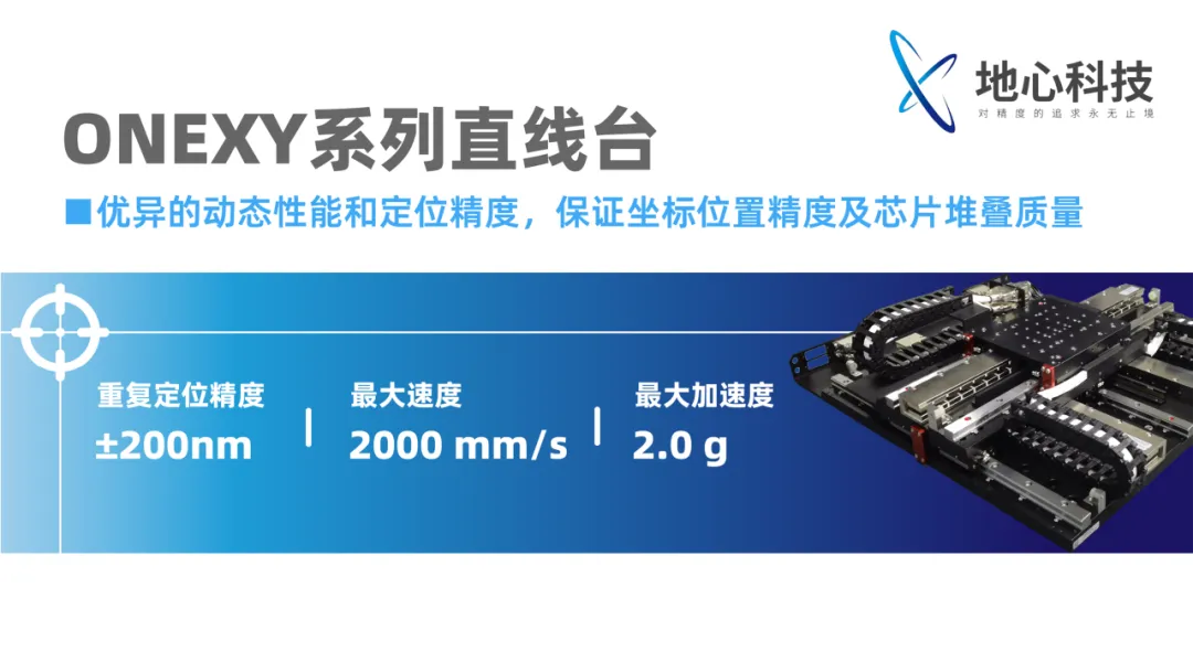
03 Back-End Packaging Process – Stacking and Bonding
This is the most critical and challenging stage in HBM production.
■ Thinning: HBM requires vertical stacking of 8, 12, or even 16 layers. The required die thickness for a 12-layer HBM is approximately 50 μm. To reach 16 layers, the thickness must be reduced to 30 μm, necessitating the grinding of wafers to an extremely thin state. This process typically employs ultra-low vibration and high-rigidity air-bearing stages to prevent ultra-thin wafers from fracturing or developing micro-cracks during processing.
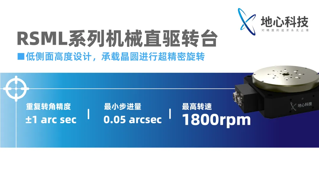
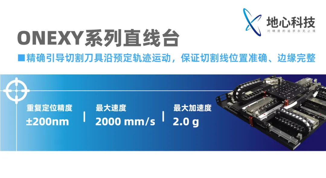
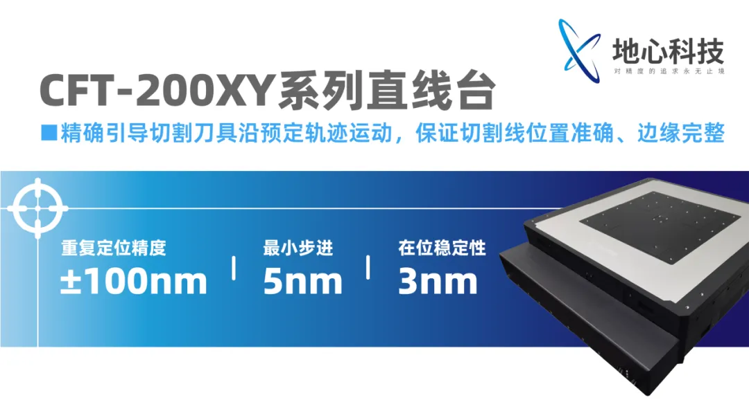
■ Die Stacking / Bonding: After precisely stacking DRAM chips layer by layer, they are connected via Thermal Compression Bonding (TCB) or Hybrid Bonding. As an advanced packaging technology that requires no solder or metal bumps, hybrid bonding perfectly addresses the core demands of HBM upgrades toward higher density, greater bandwidth, and lower power consumption.
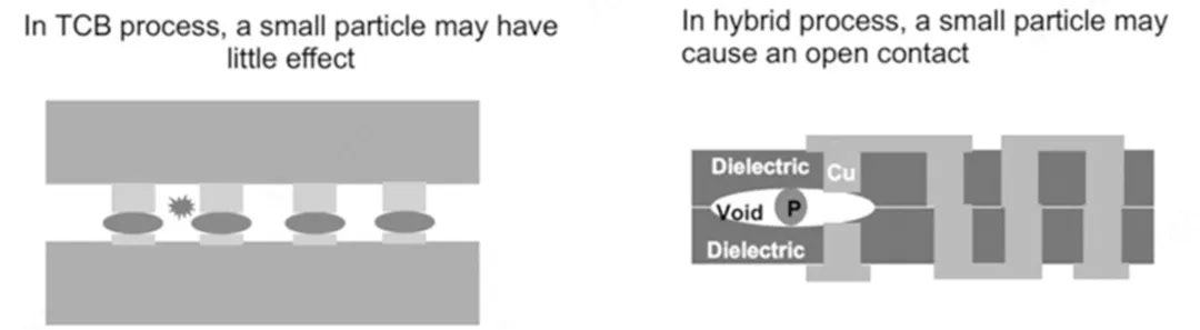
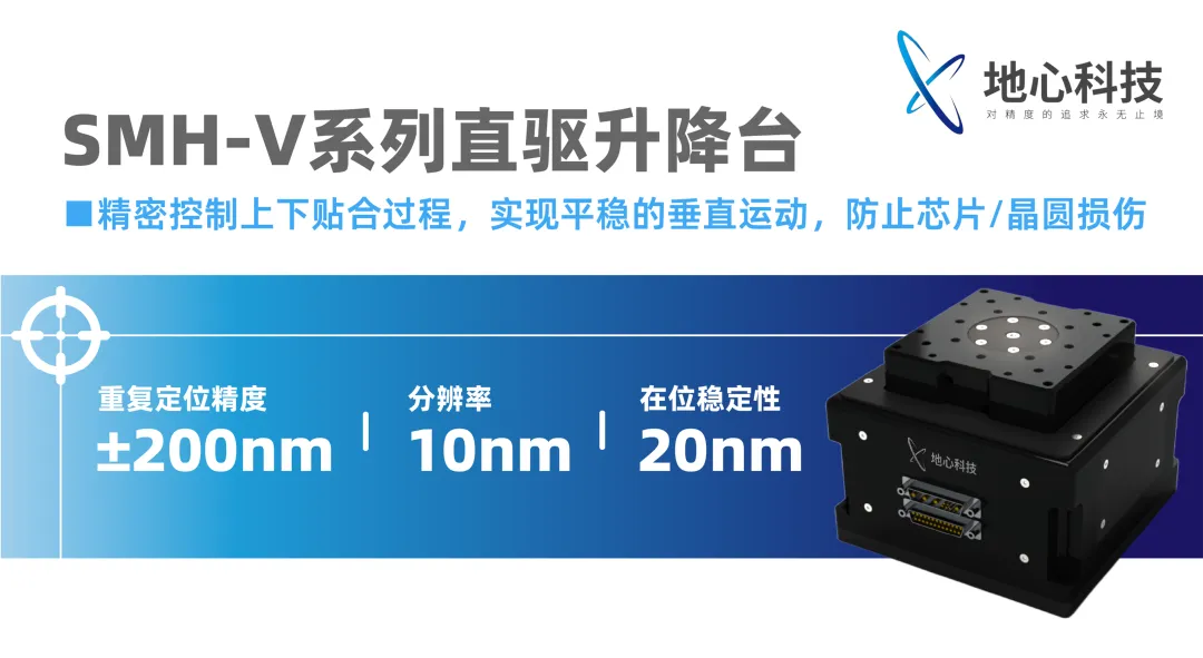
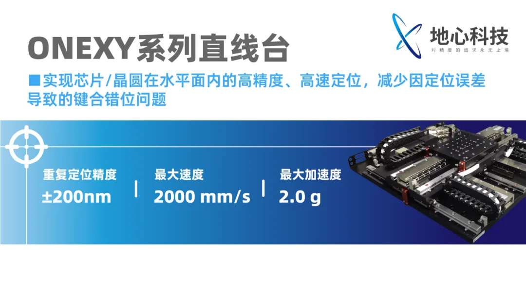
As more components and interconnections are integrated into a single package, the number of potential failure points rises. A defect in any single chip or interconnection can result in costly yield losses. In hybrid interconnection processes with chip-to-wafer bonding pitches of less than 3 μm, the bonding alignment accuracy (3σ) is typically required to be within 10% of the bonding pitch (i.e., when pitch < 3 μm, 3σ accuracy must be < 0.3 μm).
04 Inspection and Final Assembly
■ AOI Optical Inspection: On HBM mass production lines, AOI (Automated Optical Inspection) has become the dominant inspection method due to its high-speed full-inspection capability. To address HBM's complex 3D stacked structures, AOI has evolved into 3D-AOI. Its primary functions include detecting missing or bridged micro-bumps, physical tilting of stacked dies, and scratches or particle contamination on wafer surfaces.
Air-bearing high-speed scanning stages ensure minimal vibration during large-area rapid scanning, preventing interference with optical lens imaging.
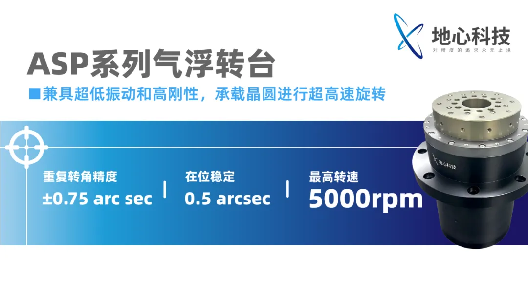
Precision requirements permeate every stage of HBM manufacturing. Particularly in the multi-layer stacking and bonding steps, tens of thousands of micron-scale bumps demand sub-micron or even nanometer-level placement accuracy and multi-axis synchronized control—factors that are central to determining stacking yield. Subsequent packaging and inspection likewise rely on precision stages to enable high-speed, accurate sorting and defect identification.
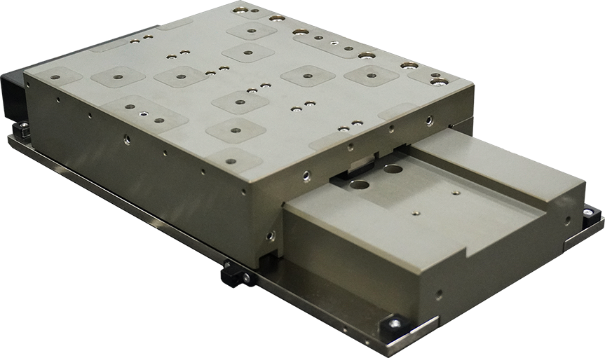
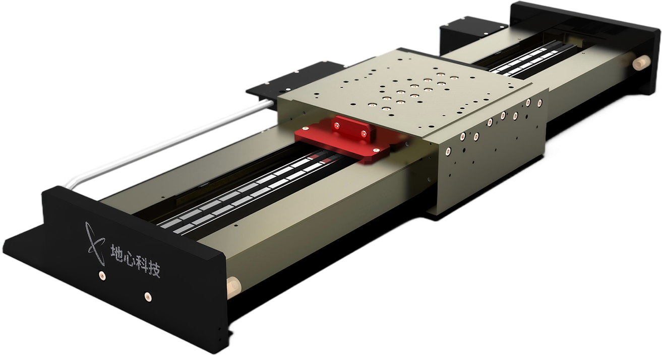
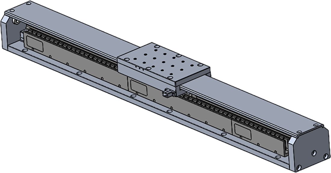
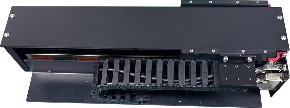
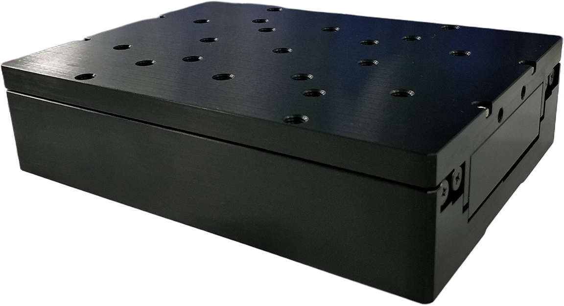
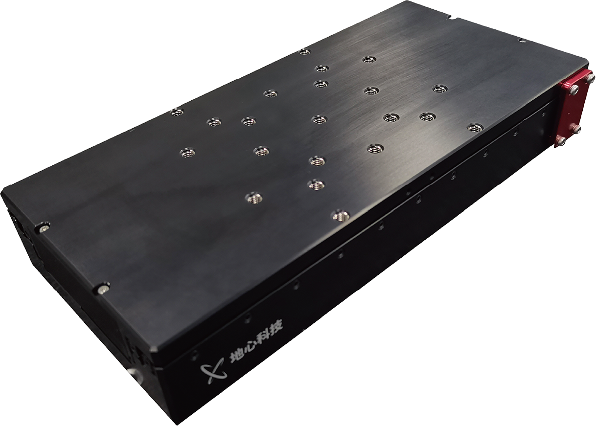
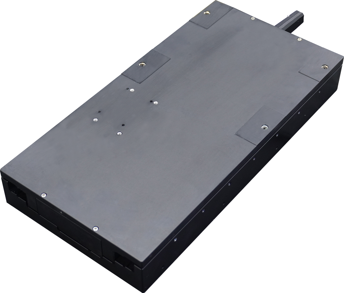
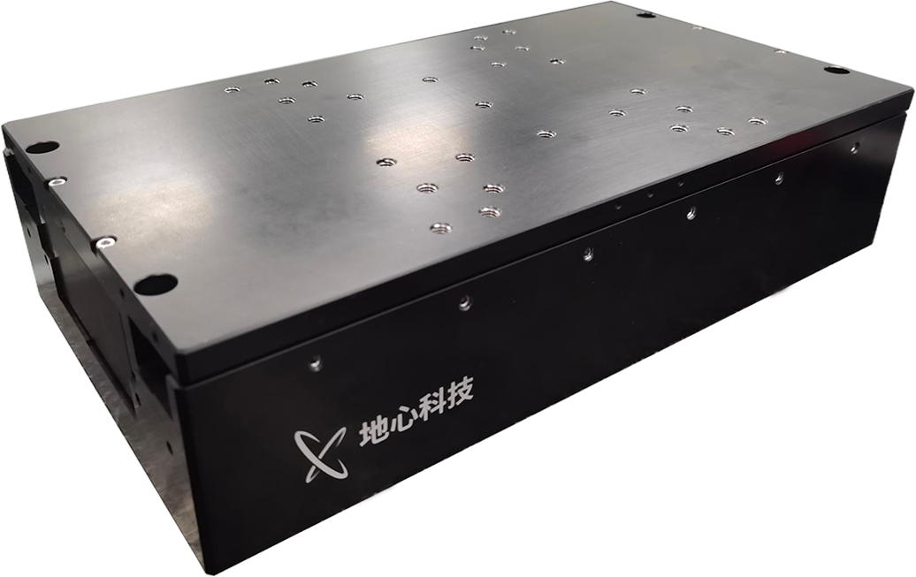
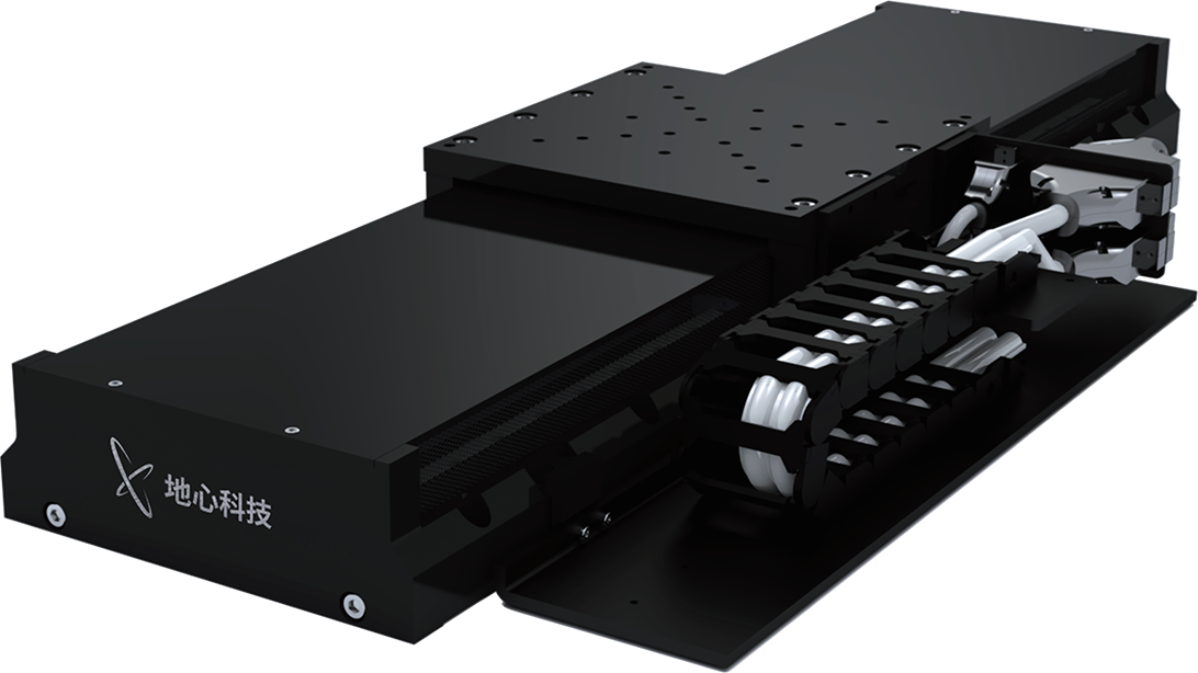
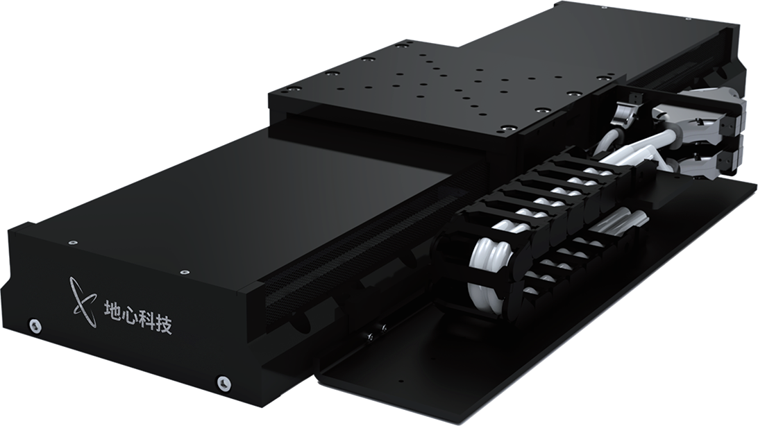
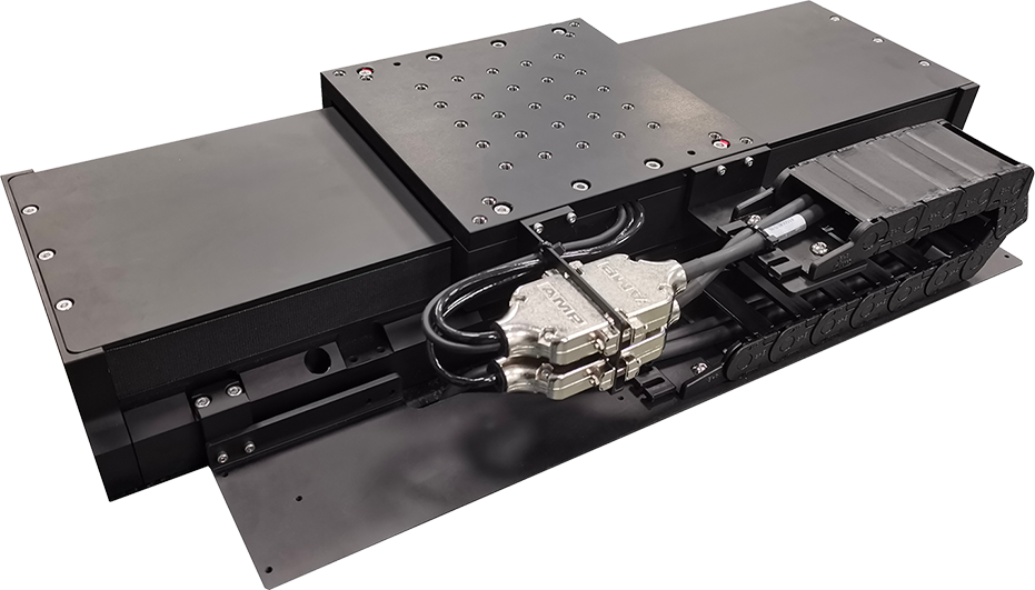
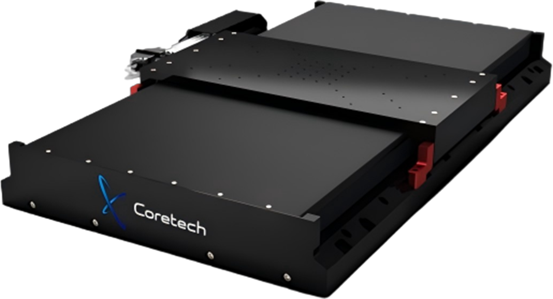
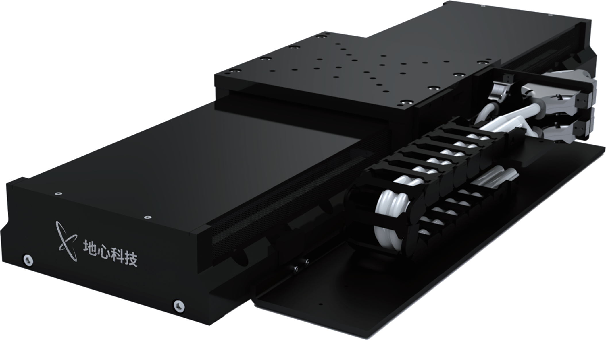
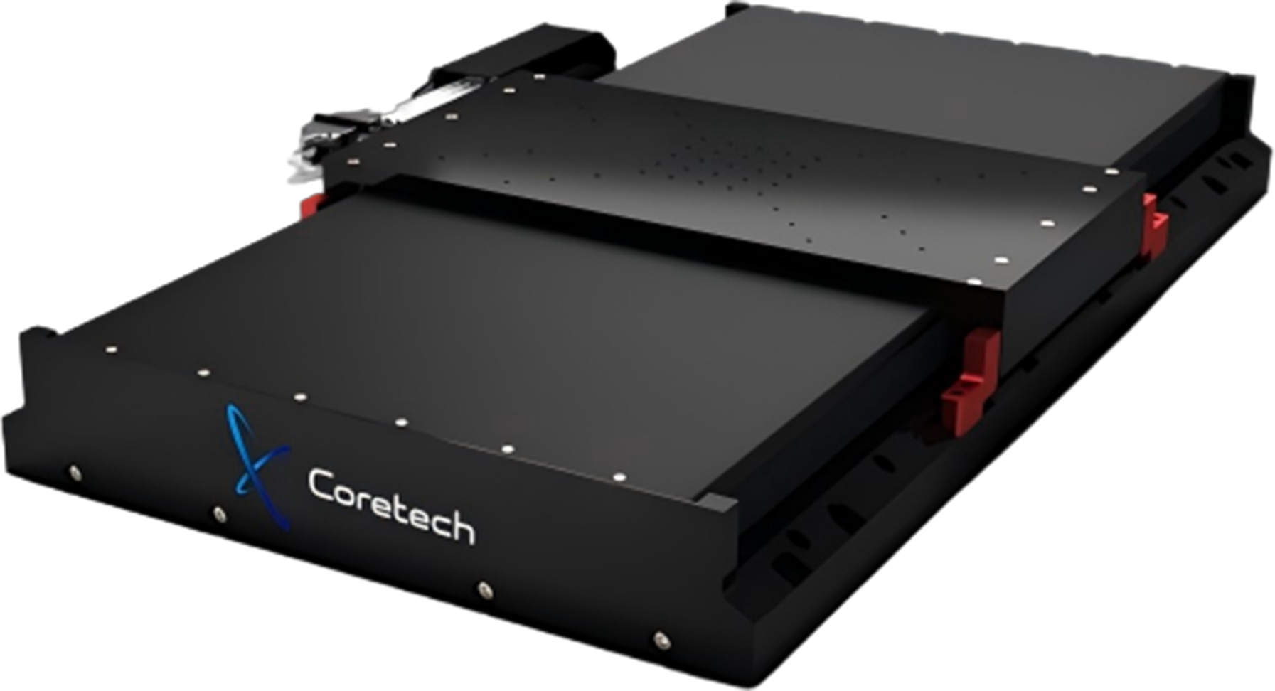
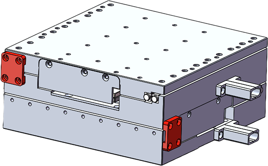
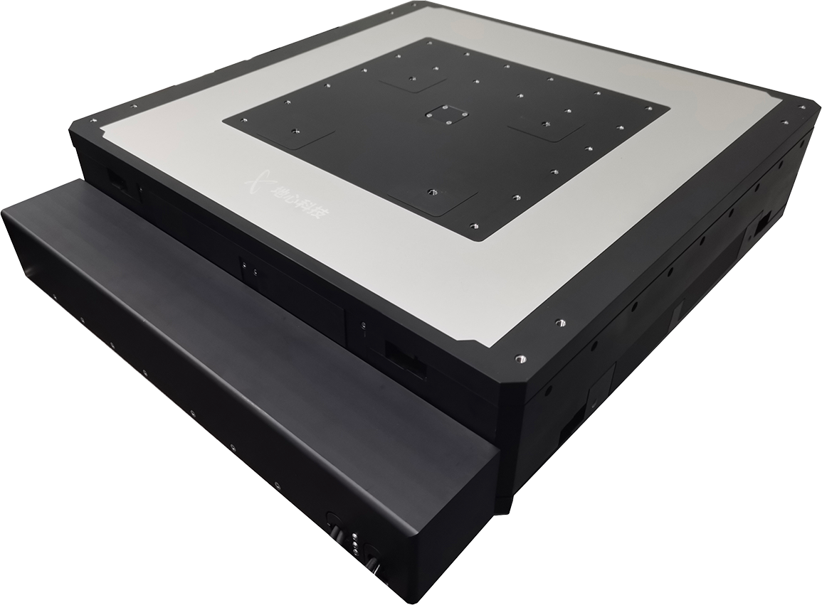
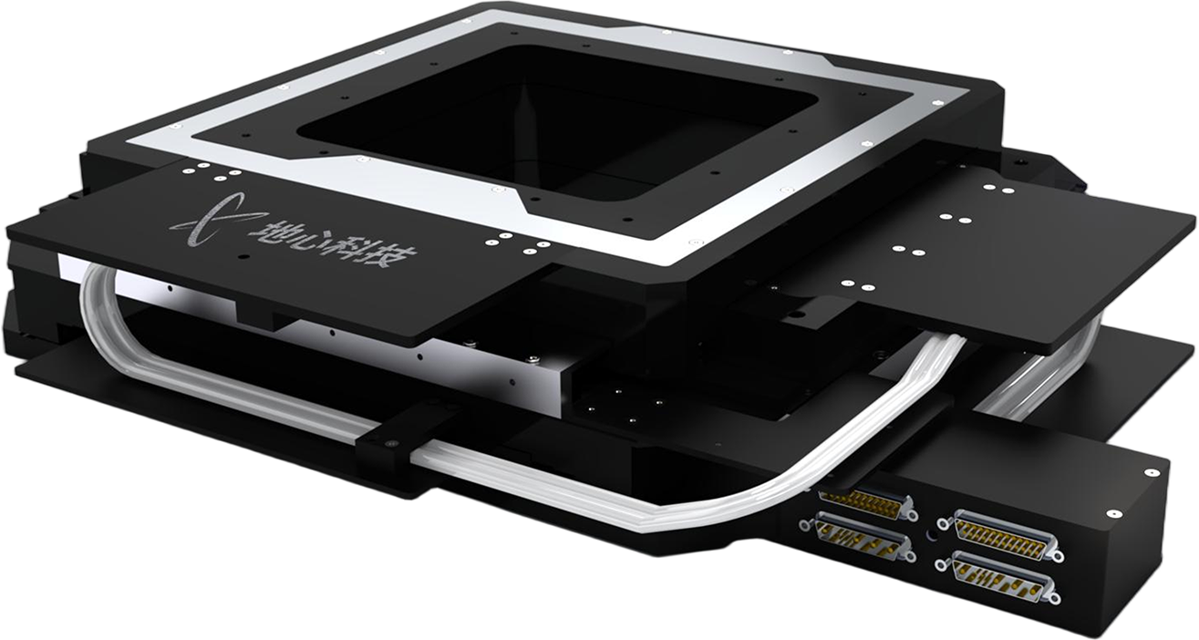
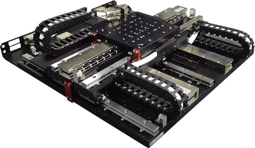
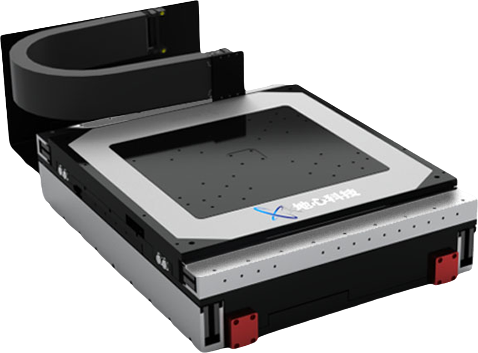
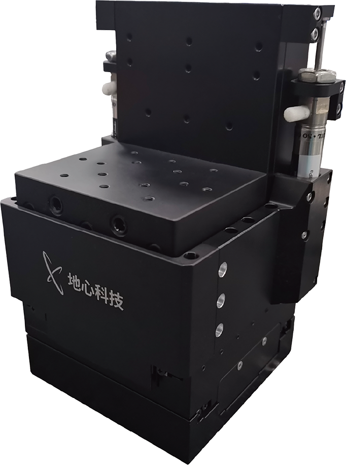
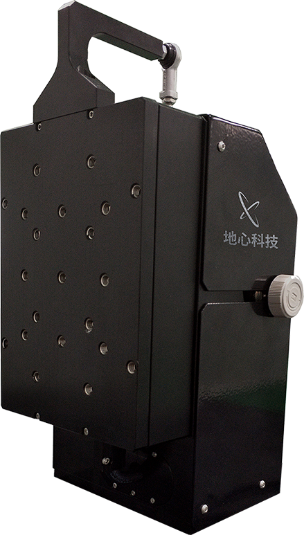
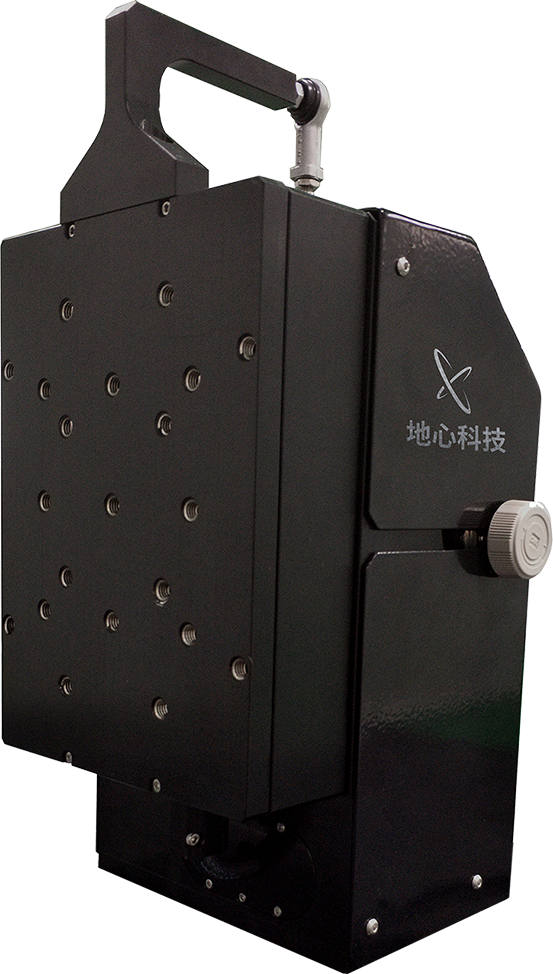
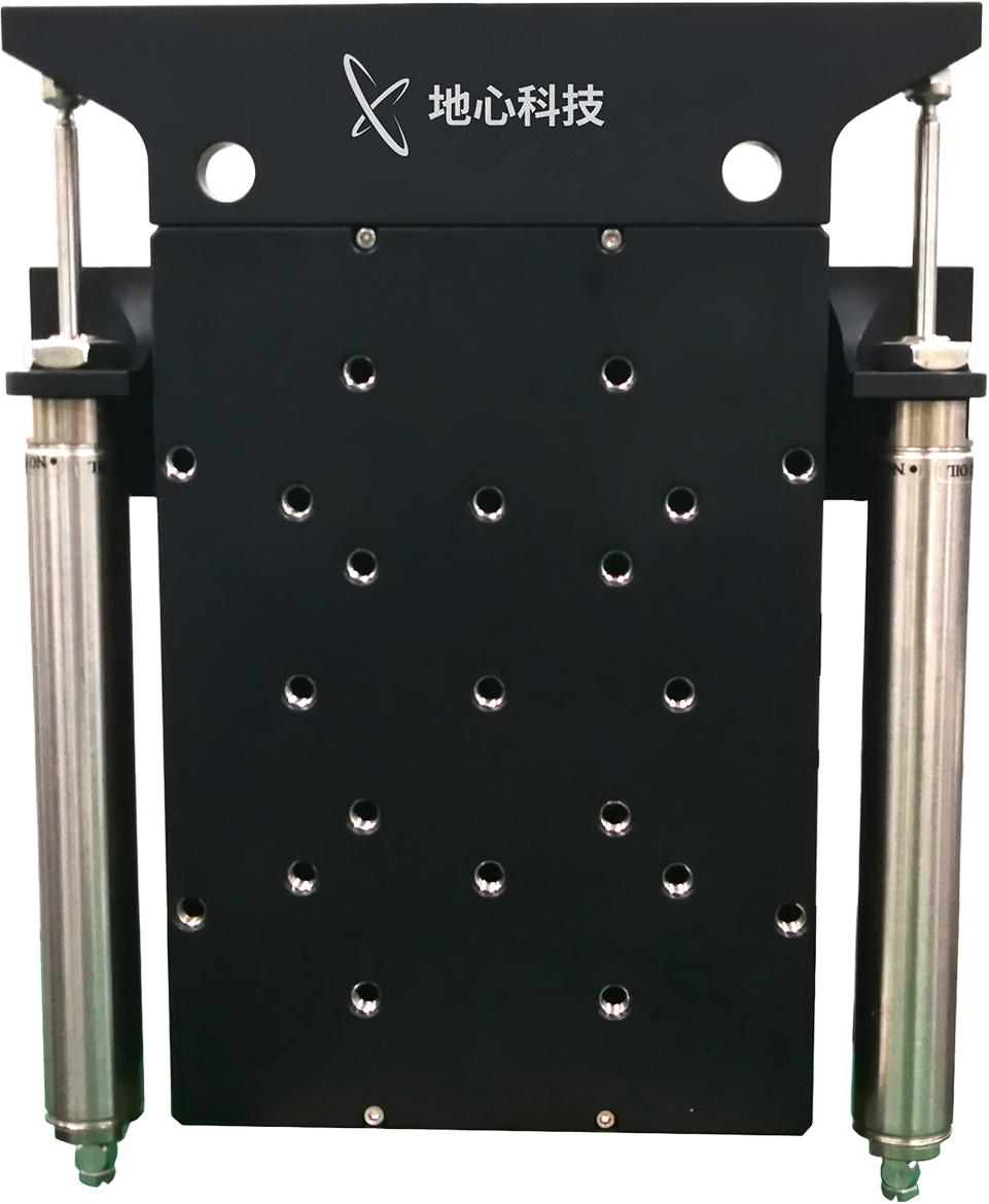
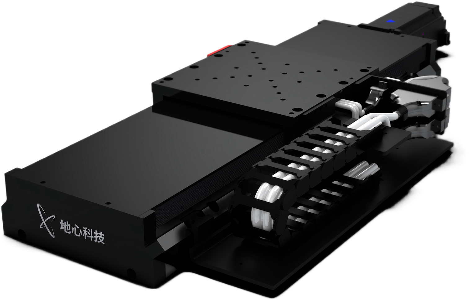
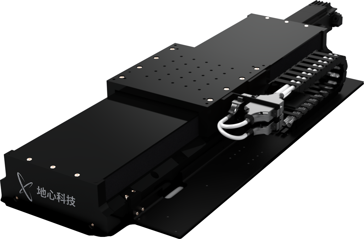
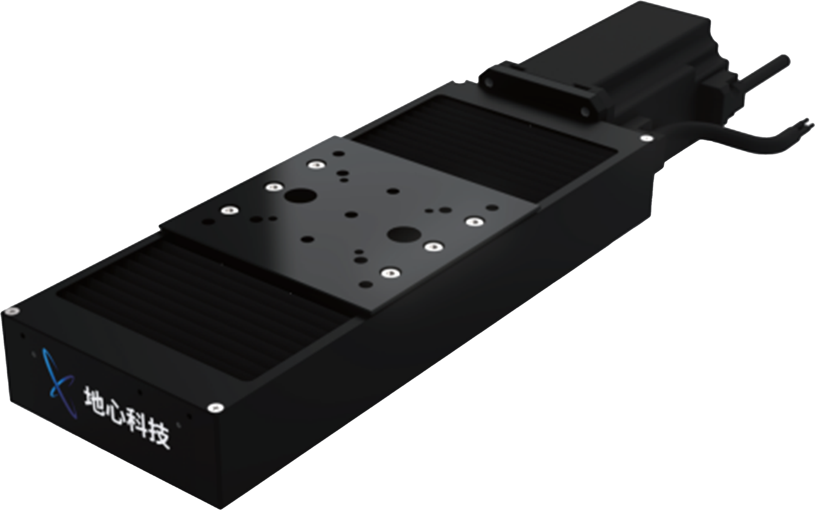
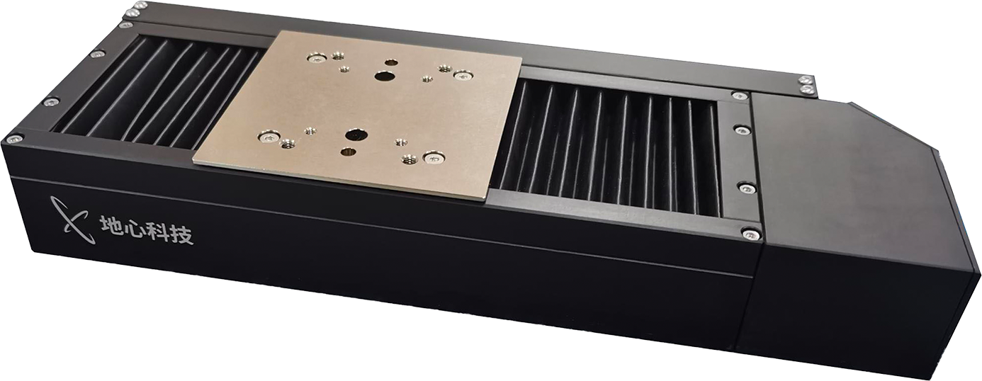
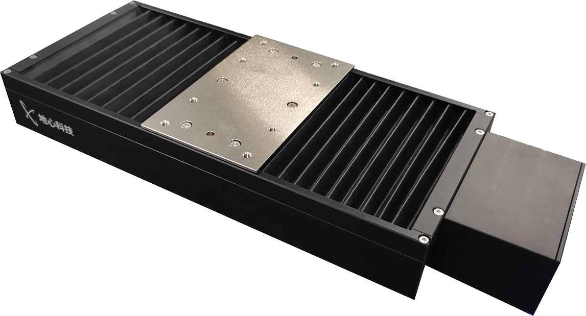
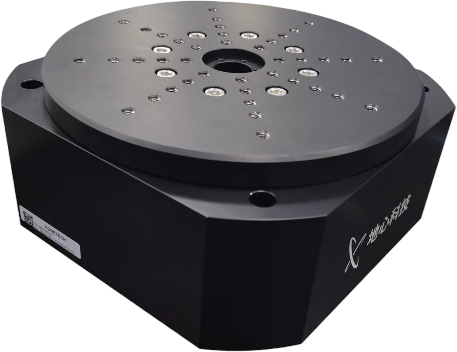
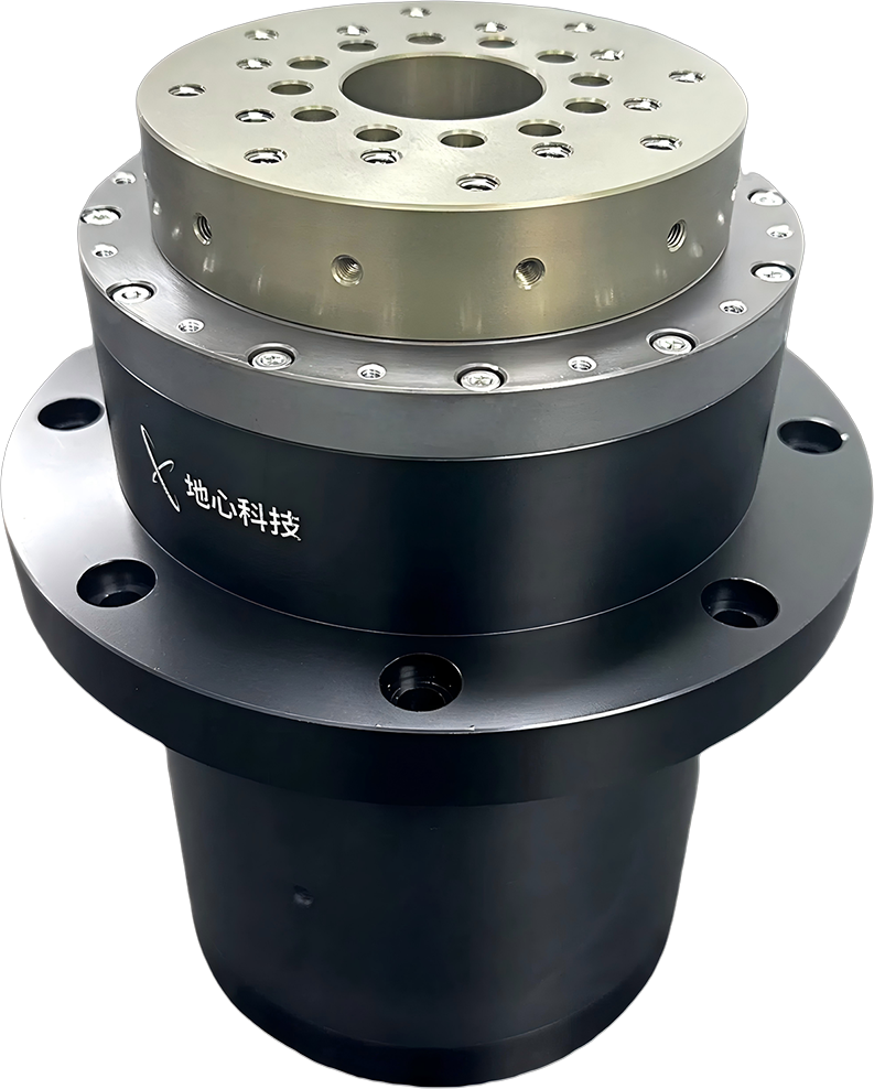
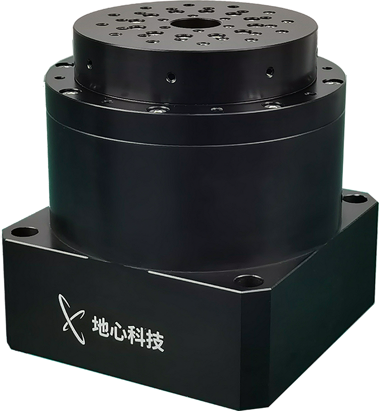
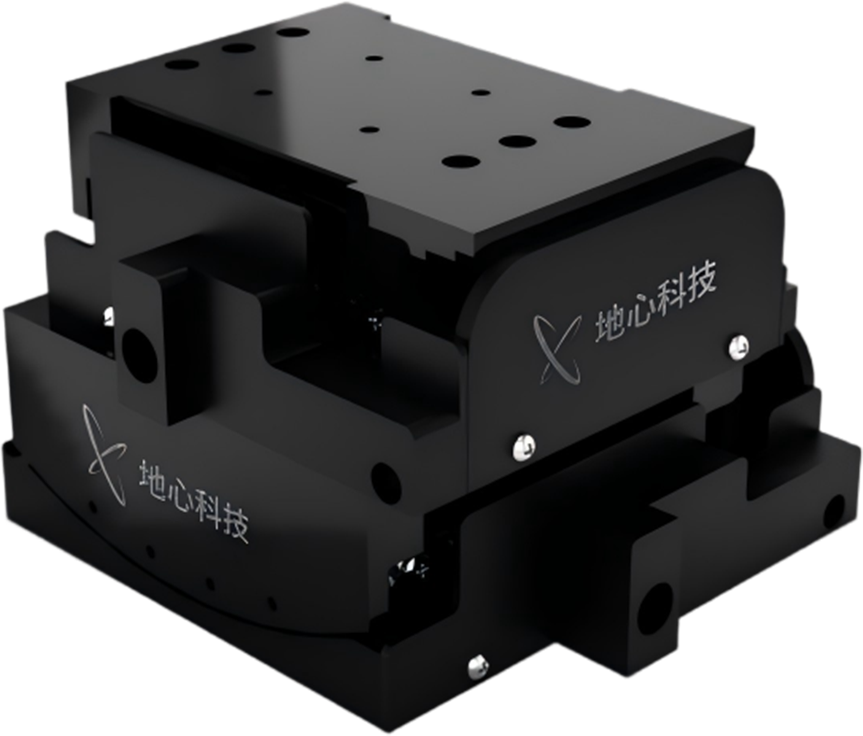
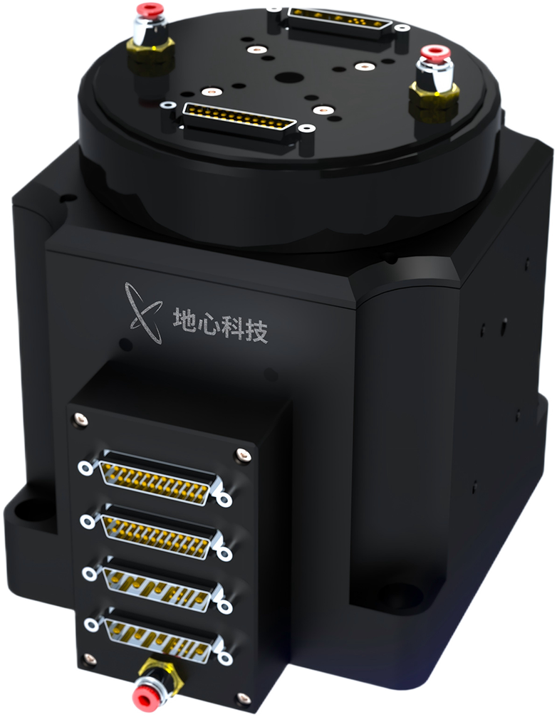
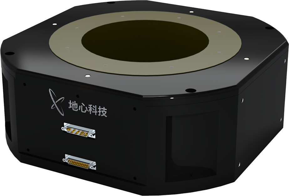
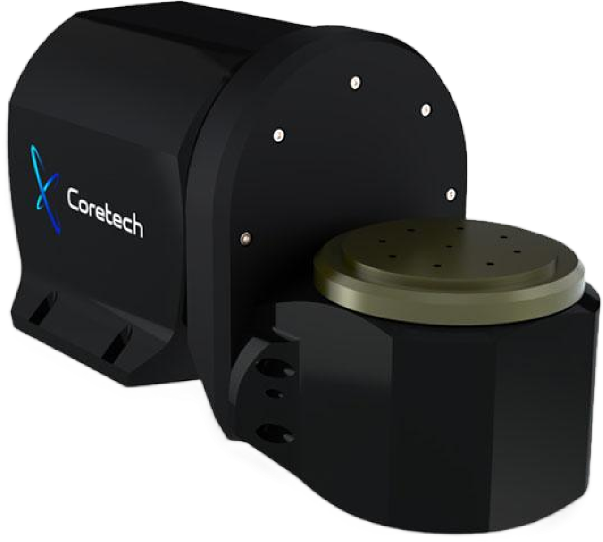
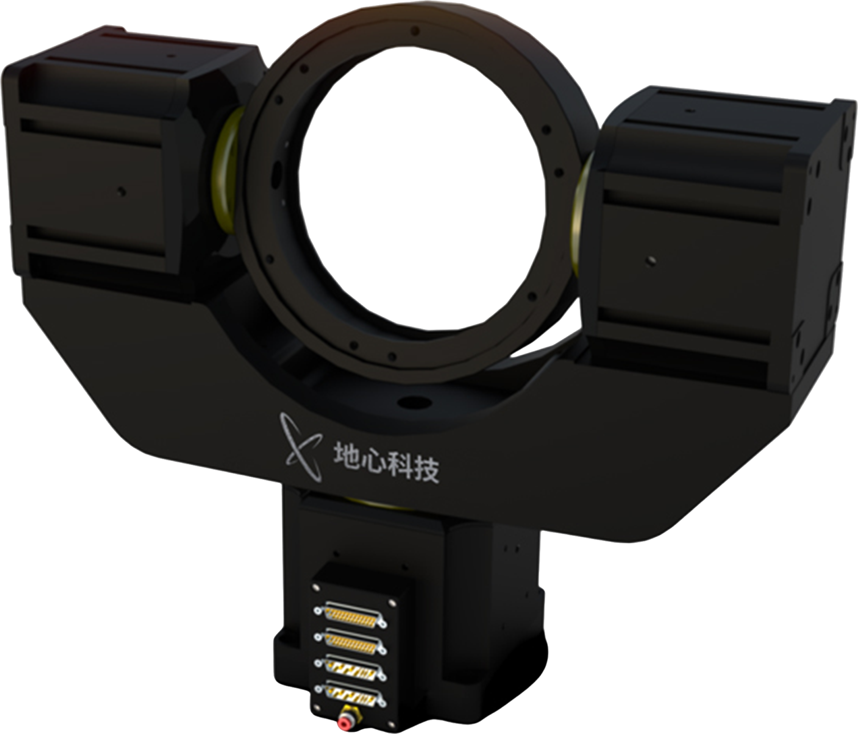
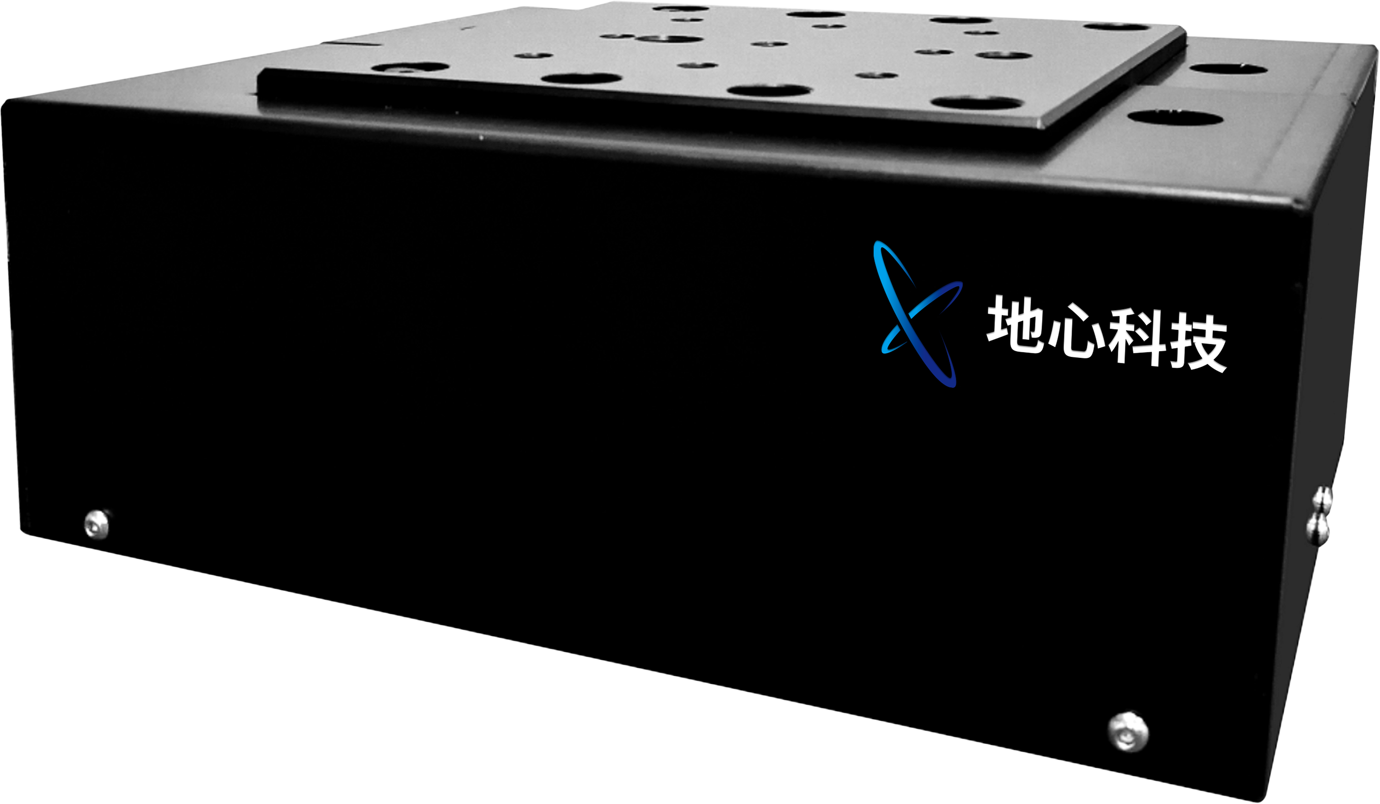
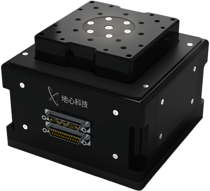
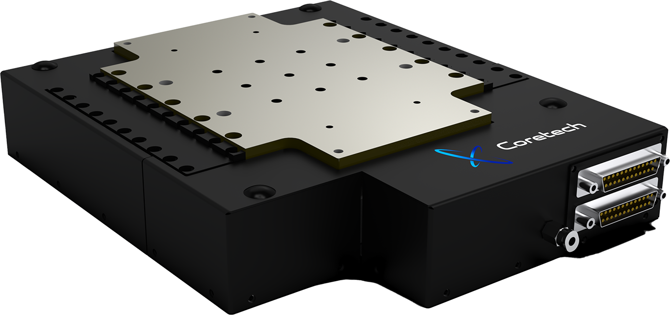
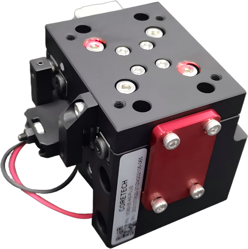
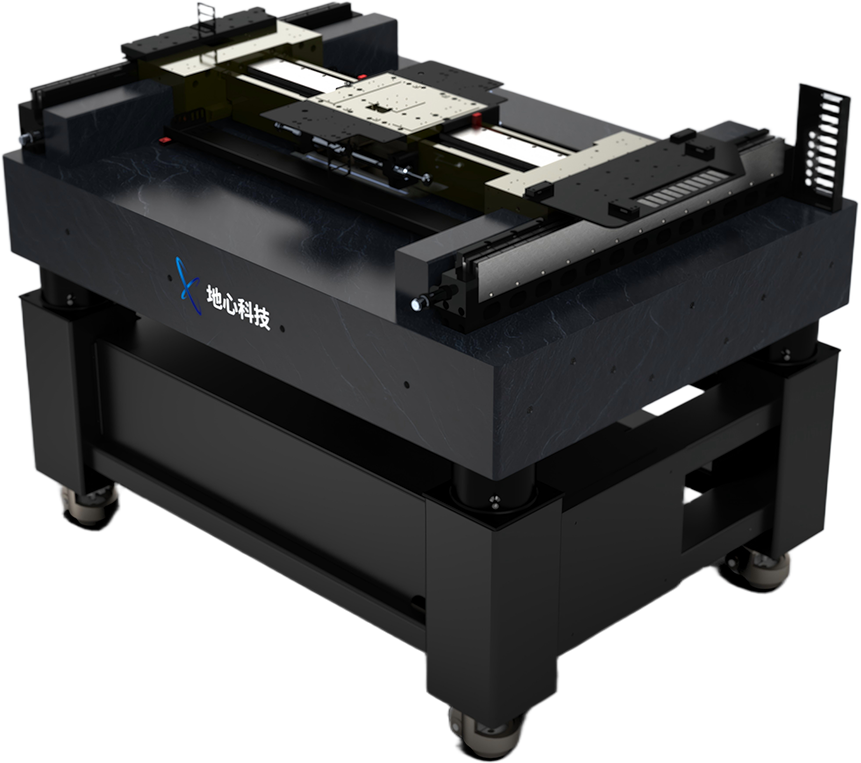
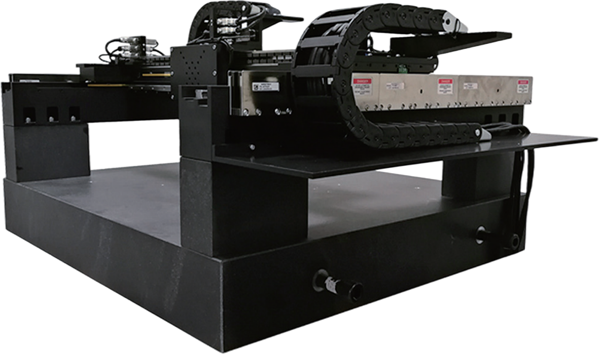
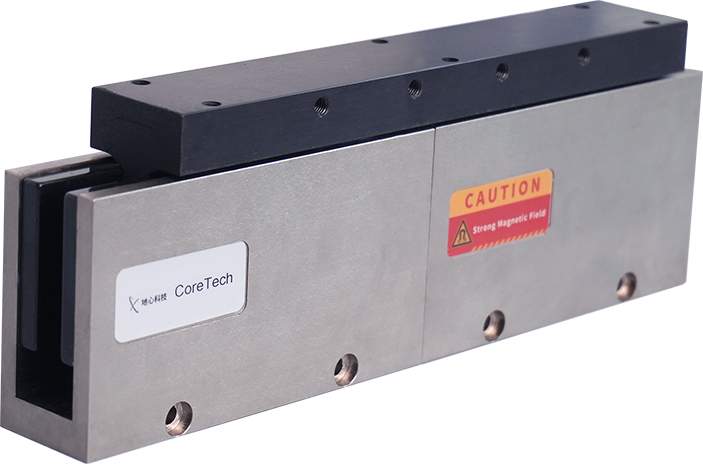
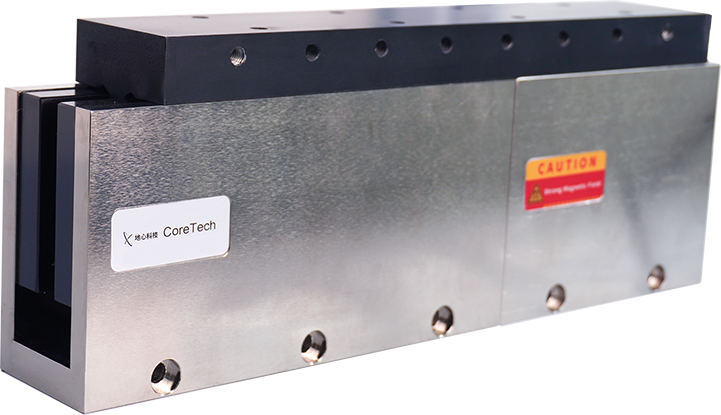
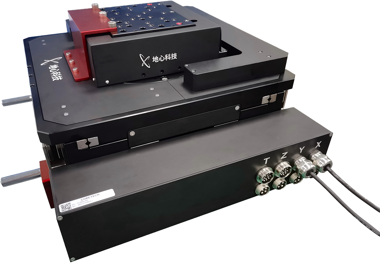
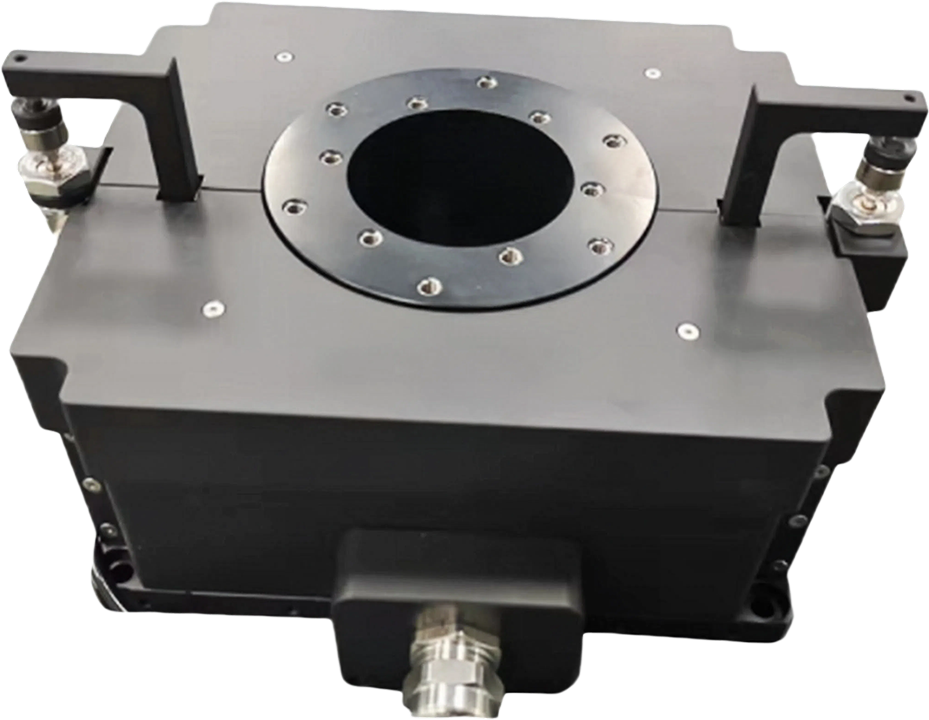
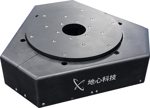
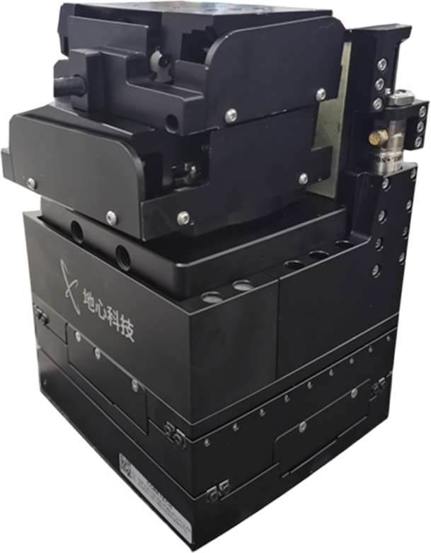
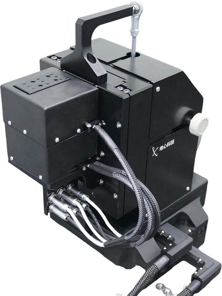
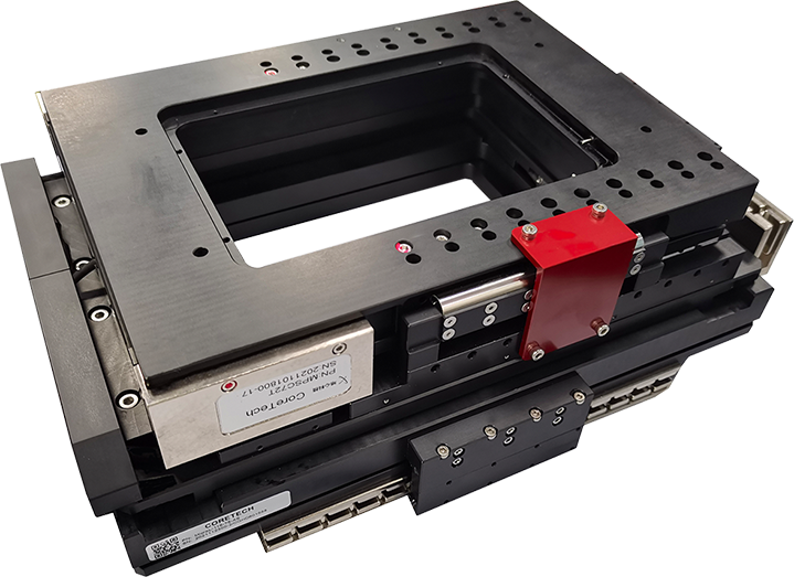
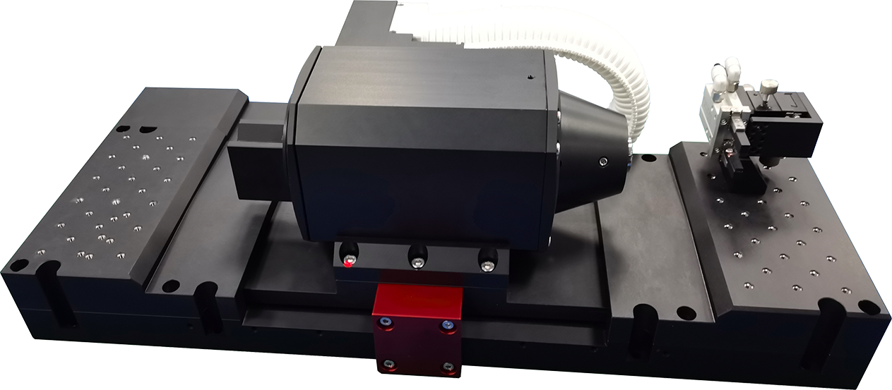
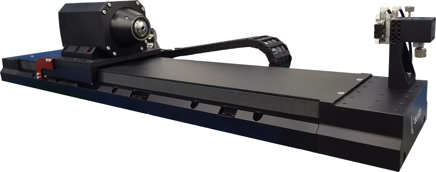
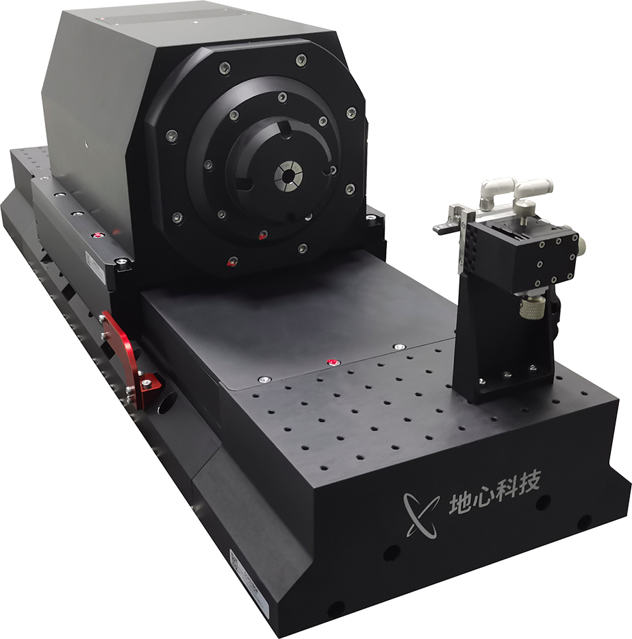
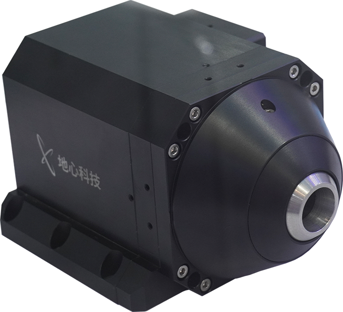
At critical nodes such as TSV lithography, ultra-thin wafer handling, multi-layer stacking bonding, and packaging inspection, Ground Motion Technology offers not just high-precision platform systems, but also application-oriented deep customization. By delivering sub-micron to nanometer-level performance while ensuring high reliability and high-value-density integrated solutions, we are proud to be a trusted partner in advancing HBM manufacturing capabilities.
Featured News
The Super Cycle of the Optical Fiber Industry Has Begun: Why Does Fiber Inspection Rely Even More Heavily on High-Precision Motion Stages?
2026.04.28
Laser Processing Automation Solutions – Laser Direct Writing and Plate‑Making Lithography
2026.06.03
Laser Processing Automation Solutions – Stent Laser Cutting
2026.06.03
 Back to List