
.png)

.png)







Home
 News Center
Coretech Application | Large Aperture 2D Motion Stage Enhances Reticle Inspection Accuracy in Mask Lithography
News Center
Coretech Application | Large Aperture 2D Motion Stage Enhances Reticle Inspection Accuracy in Mask Lithography
News Center
Coretech Application | Large Aperture 2D Motion Stage Enhances Reticle Inspection Accuracy in Mask Lithography
Coretech Application | Large Aperture 2D Motion Stage Enhances Reticle Inspection Accuracy in Mask Lithography
 2026-06-03
Share:


"Coretech's CFTCA series high-precision large-aperture 2D motion stage is widely used in microscopic imaging equipment, particularly in photomask/reticle inspection applications for lithography, thanks to its outstanding stability and minimum step capability."
01 Lithography Technology
Lithography is a critical technology commonly used in semiconductor manufacturing processes. It involves projecting designed chip patterns onto semiconductor material surfaces using a lithography system, followed by a series of processing steps, ultimately forming micron- and nanometre-scale chip structures.
The fundamental principle of lithography utilises the properties of light—through a light source, mask, photosensitive material, and development steps—to transfer patterns onto a substrate to be processed. Light passes through the transparent regions of the mask and irradiates the photosensitive material, inducing chemical or physical changes. The unexposed photosensitive material is then removed through development, ultimately forming the desired pattern. ASML is a well-known major manufacturer of lithography systems.
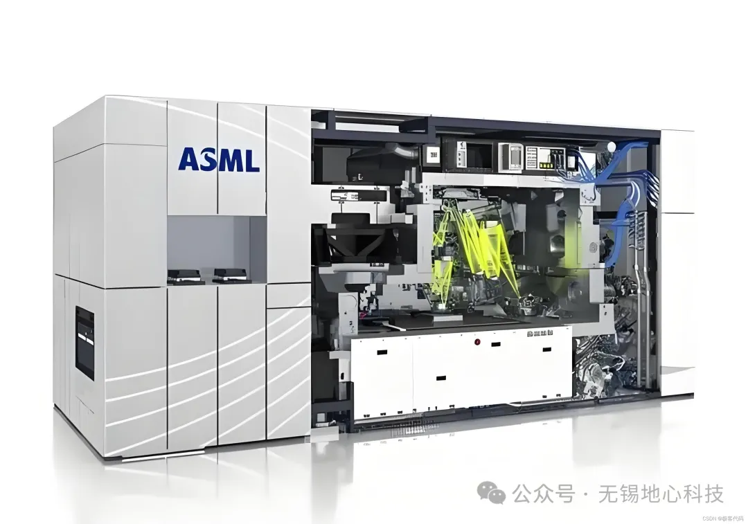
The basic principle of lithography includes the following steps:
Mask fabrication: A desired chip pattern is created on a transparent substrate and overlaid onto the semiconductor material.
Photoresist coating: A layer of photoresist is applied to the surface of the semiconductor material. The choice of photoresist depends on the wavelength and energy of the light source.
Exposure: The lithography system projects UV light carrying the chip pattern through the mask onto the photoresist. The exposure process causes chemical or physical changes in the photoresist within the illuminated areas.
Development: The chemical changes make the exposed photoresist soluble in a corresponding developer solution, while the unexposed areas remain unchanged, forming a lithographic pattern.
Pattern transfer: Using chemical or physical methods—such as shallow etching or doping—the lithographic pattern is transferred to the semiconductor material surface.
Process iteration: The above steps are repeated in successive iterations until the final chip structure is achieved.
02 Reticle/Photomask Inspection
A photomask (also referred to as "reticle," "mask," "photomask," or "light shield") is typically made of glass or quartz with a patterned metal layer on its surface that selectively blocks or transmits light. It is an essential tool in the microelectronic lithography process.
The mask is an indispensable component of lithography. It carries the designed circuit pattern; light passes through it, projecting the pattern onto the photoresist. The mask functions analogously to the "negative" in traditional photography. By creating patterns on the mask, the pattern is transferred to the substrate through subsequent exposure processes, forming the corresponding circuit features on the substrate.
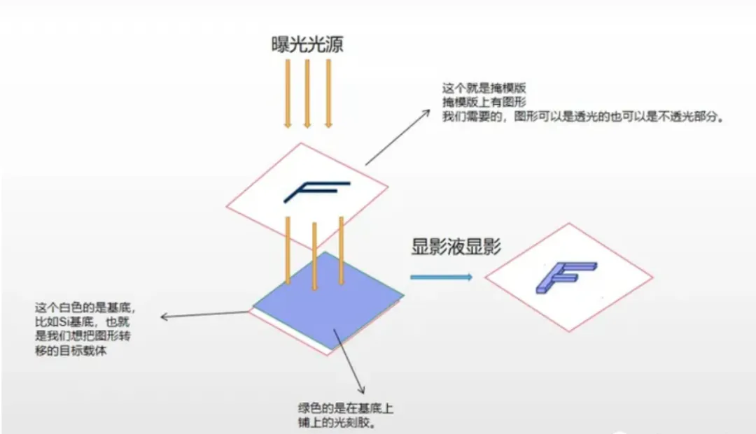
Defects in photomasks can arise from various sources, including pattern fabrication defects in the mask itself, particle inclusions in the resist or cleaning solutions, debris from equipment chambers, or defects on blank masks. Any defect larger than one-quarter of the minimum feature size on the mask may lead to device failure on the wafer.
Inspection of photomasks primarily falls into the following categories:
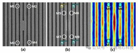
Macroscopic inspection: Using light sources of different wavelengths and intensities to visually (macroscopically) inspect the mask surface for defects (Defect), mura, particles, and other anomalies.
Automated Optical Inspection (AOI): Using light sources of specific wavelengths and intensities to acquire the pattern of the product under inspection, capturing the illuminated image via sensors (cameras) and digitising it. The image is then compared, analysed, and evaluated through dedicated logic and software algorithms to detect surface defects such as line opens (Open), line shorts (Short), white protrusions (Intrusion), and missing patterns.
Precision measurement and calibration: Using high-precision measurement equipment to measure line/space (CD) accuracy and uniformity, total pitch (TP) accuracy, and registration (positional) accuracy of the mask pattern, confirming that the product meets required specifications. Additionally, based on measurement results and related algorithms, corrections and compensations are applied to the mask and stage platform to meet product requirements.
03 Coretech Products
Coretech has many years of application experience in the semiconductor industry. A variety of product combinations can meet the needs of different users. From wafer scribing/dicing, wafer defect inspection, wafer film thickness measurement, to die attach and soldering, Coretech offers excellent solutions across multiple process stages. Over many years of deployment, the company has not only accumulated extensive application experience but has also earned a strong reputation.
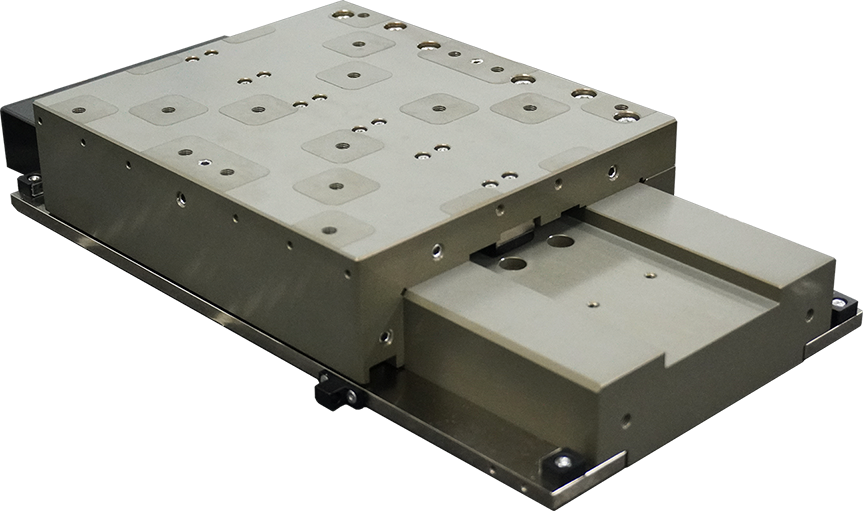
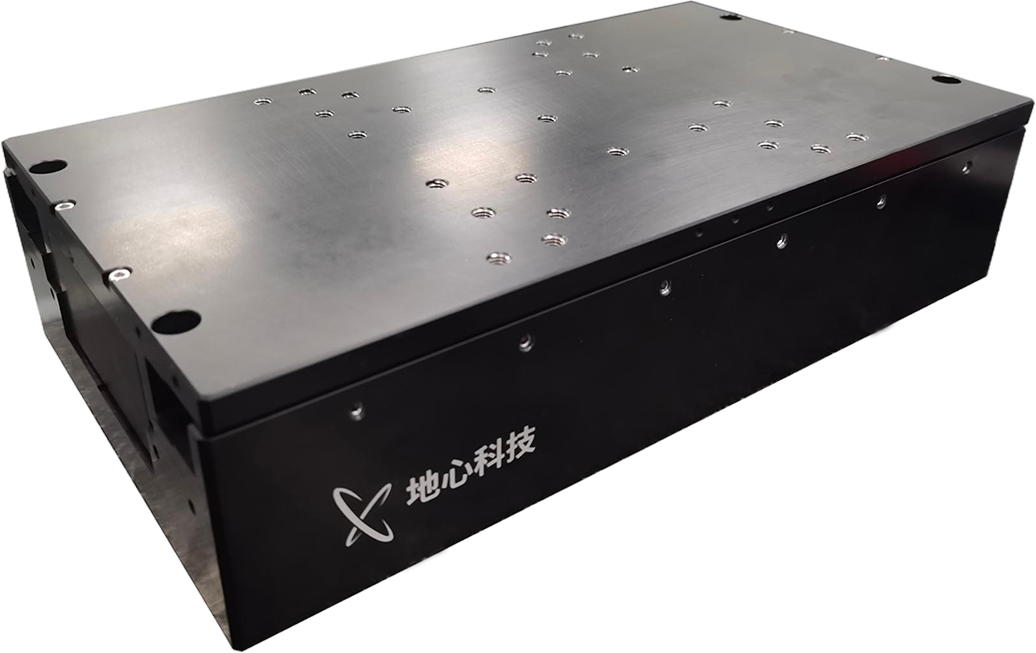
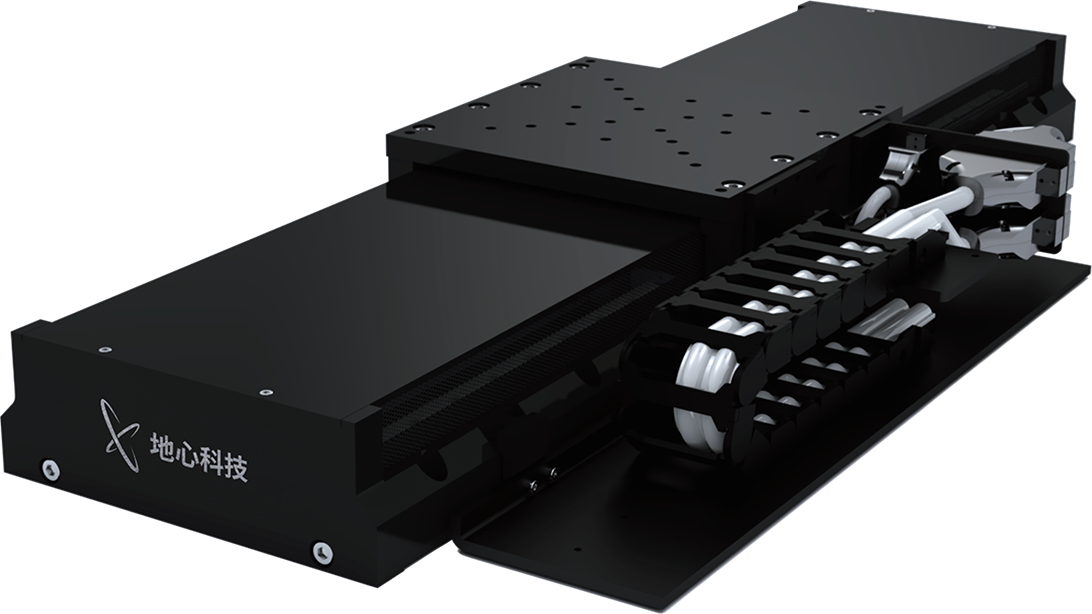
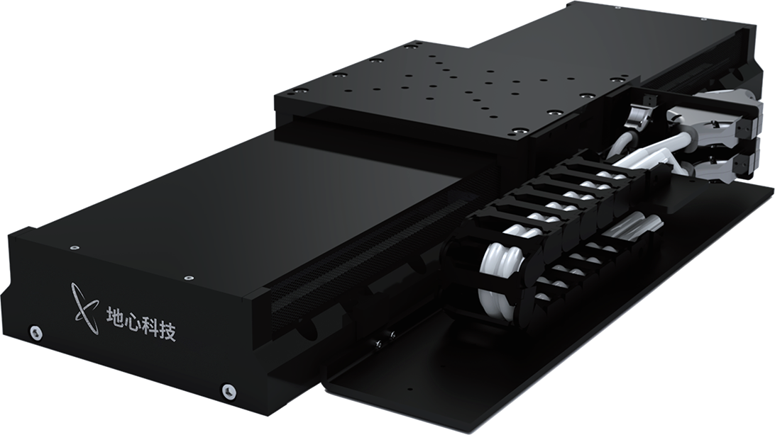
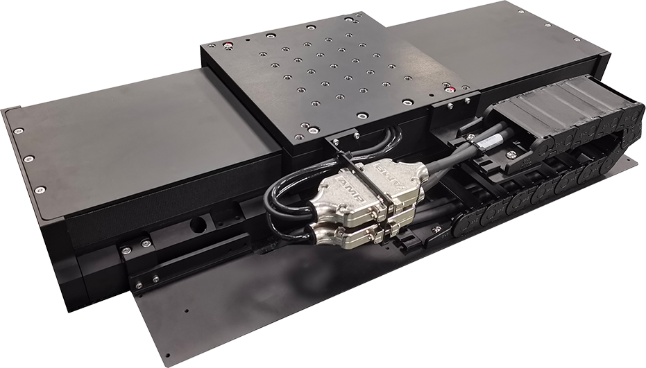
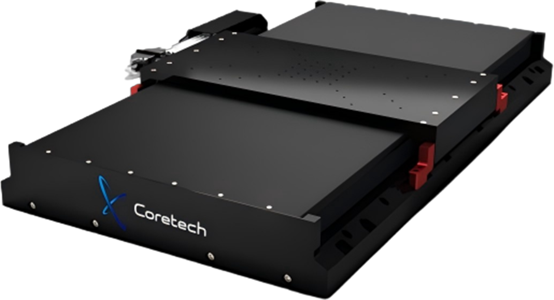
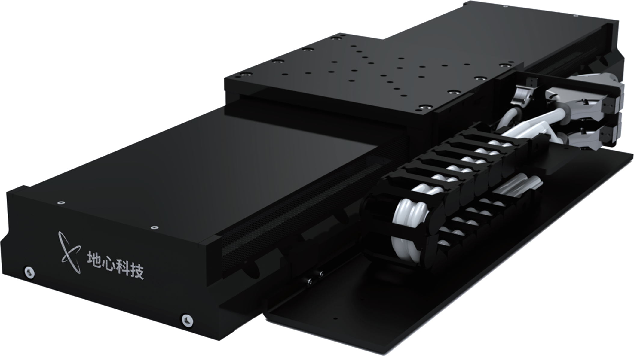
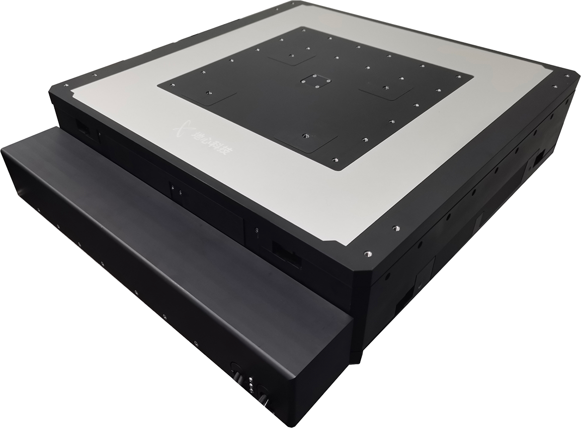
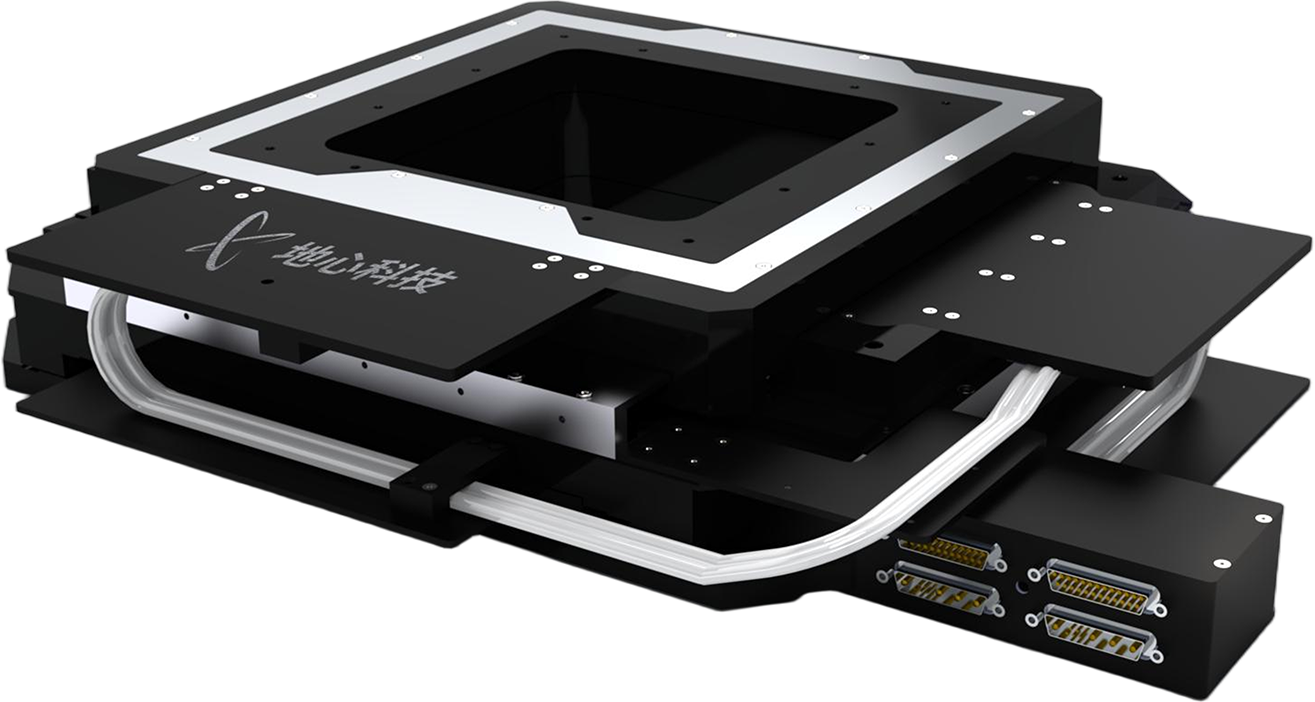
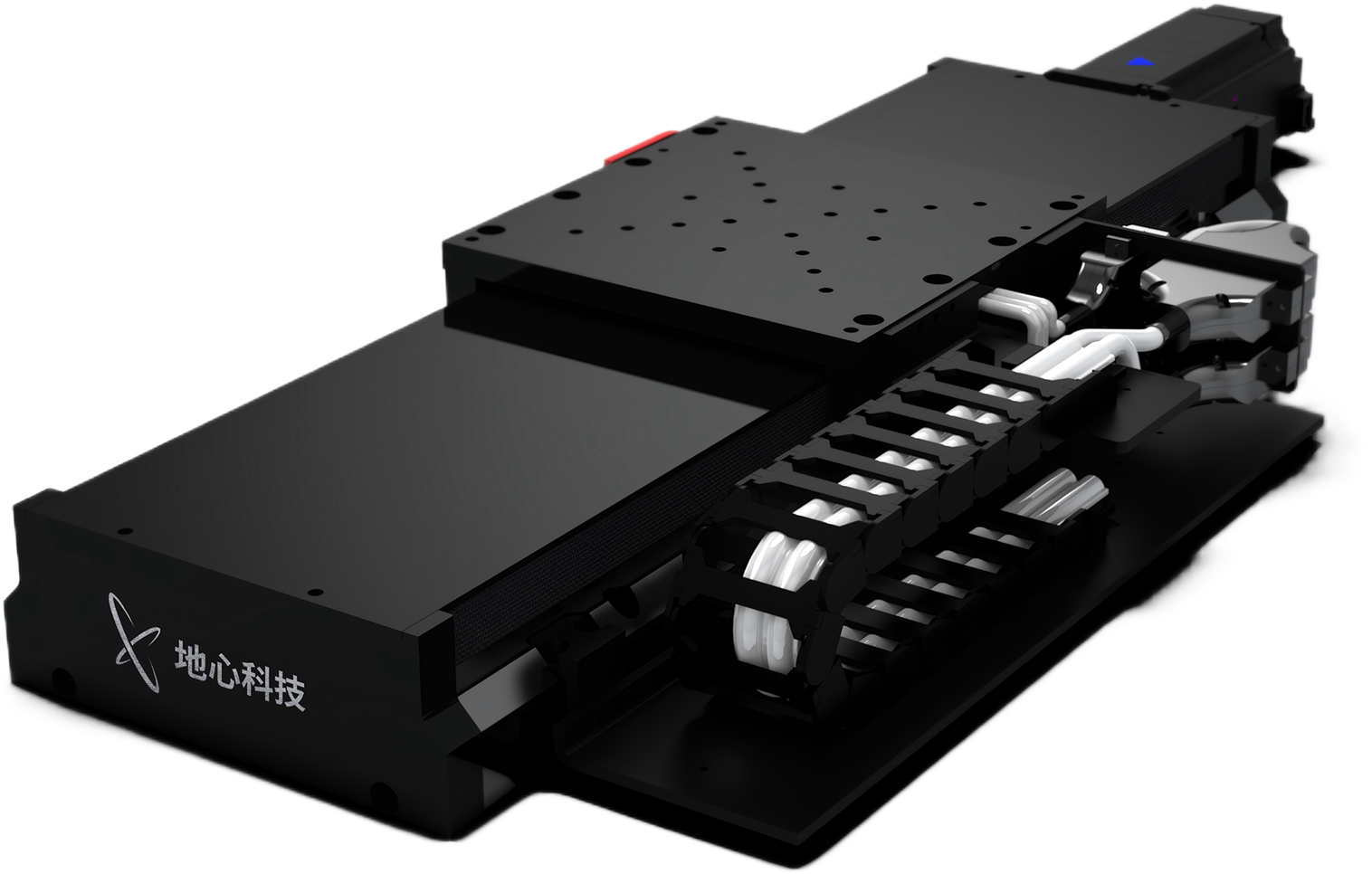
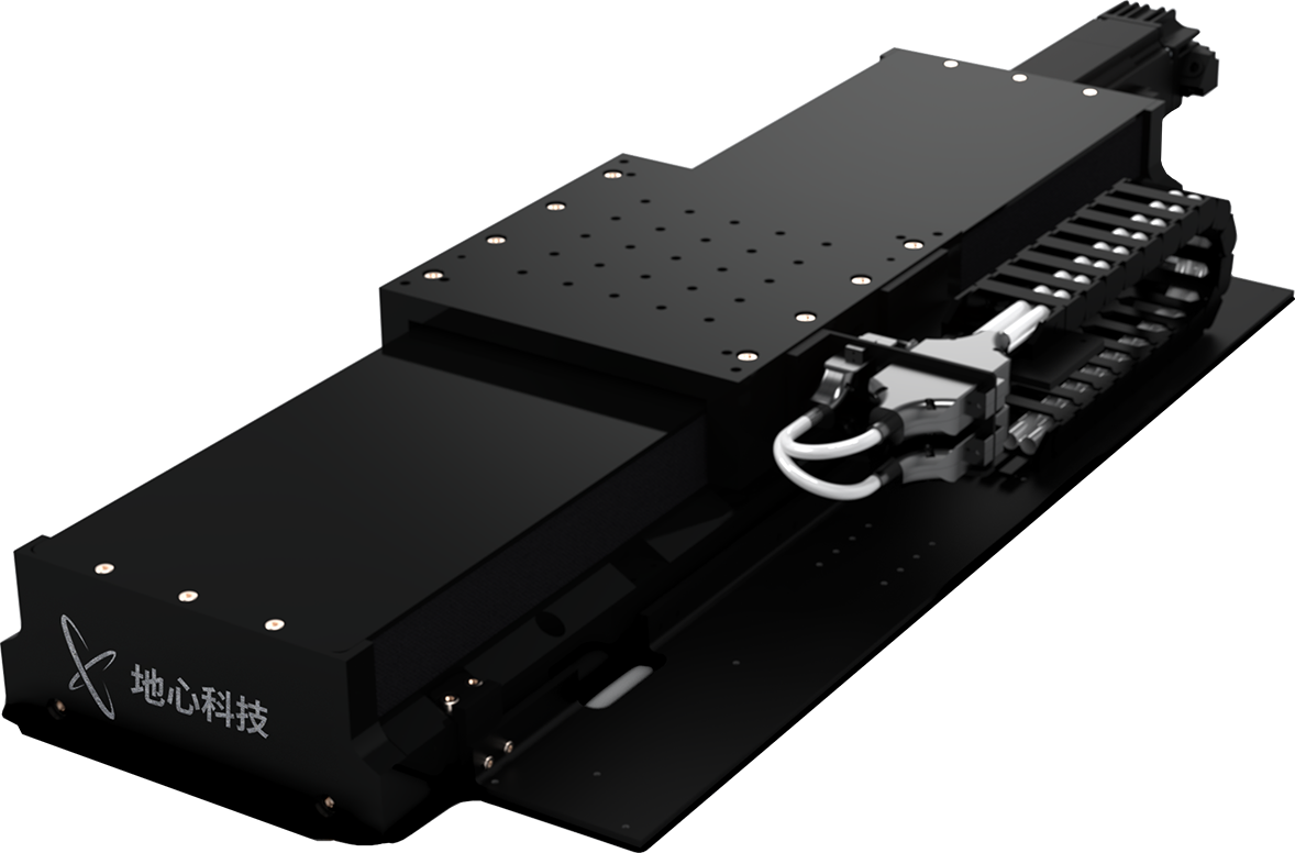
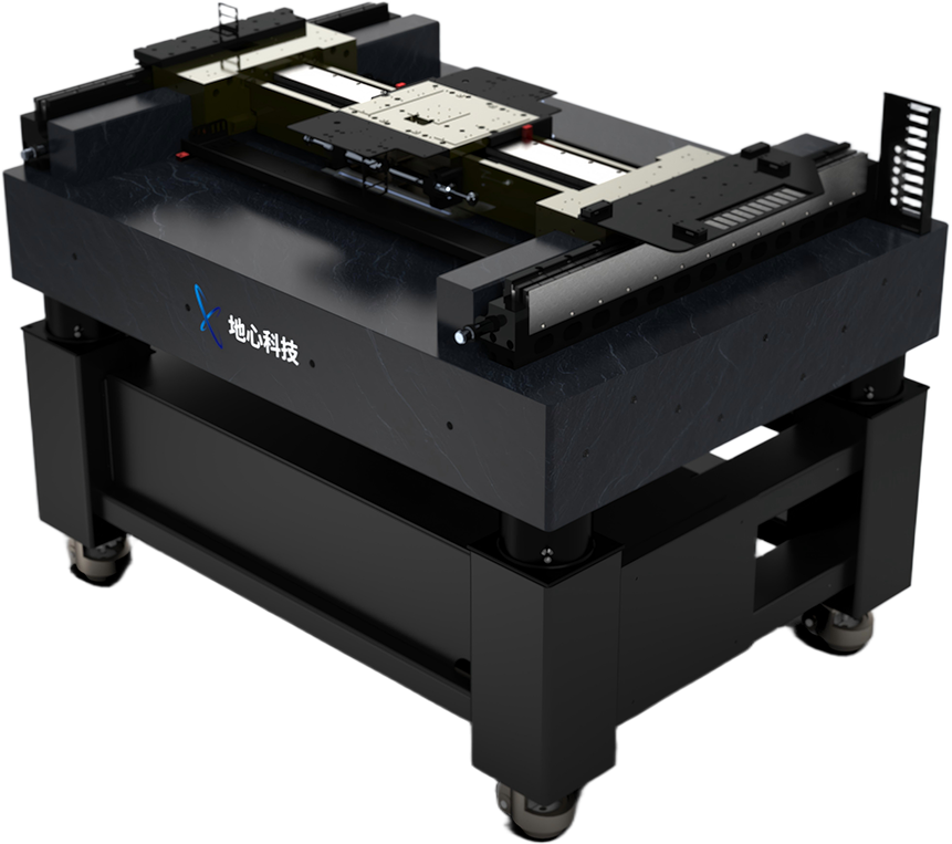
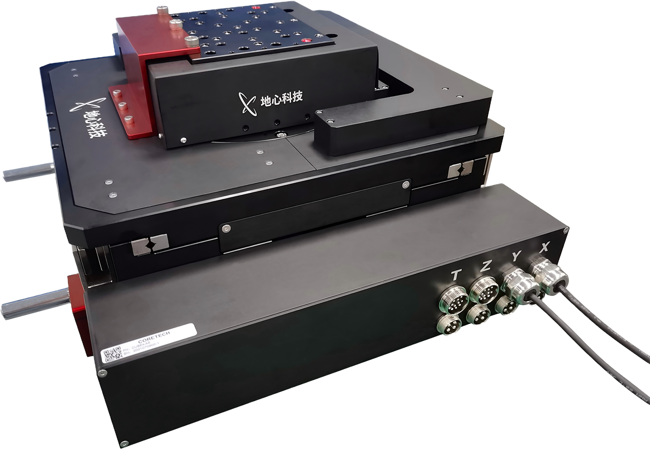
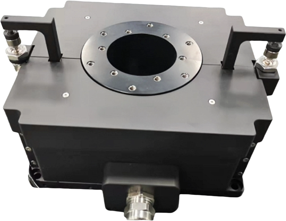
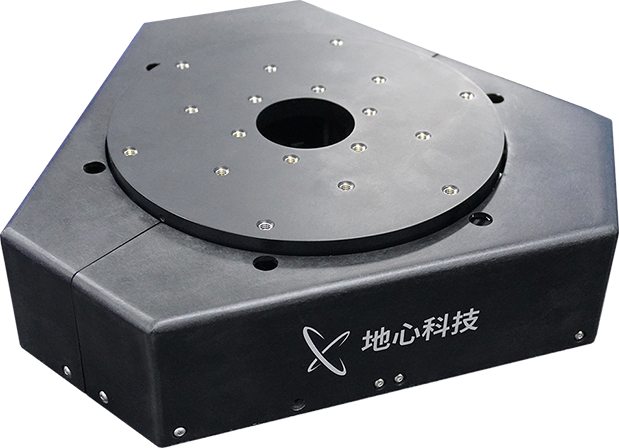
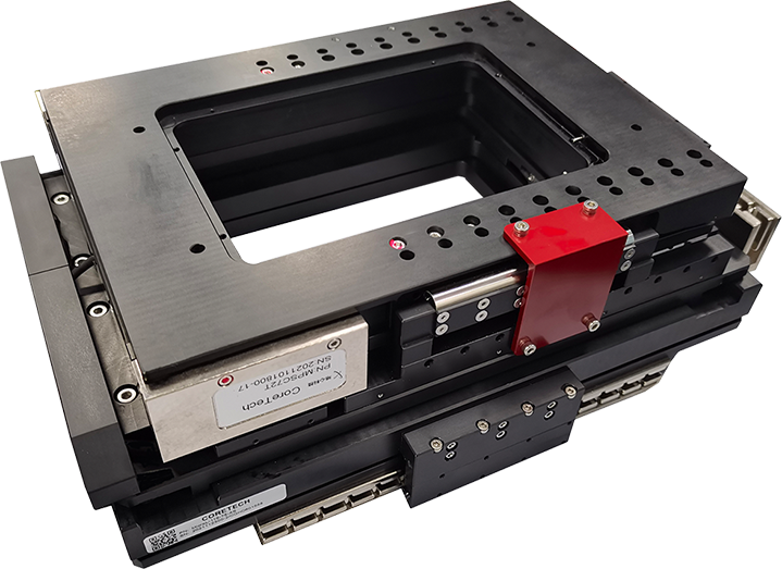
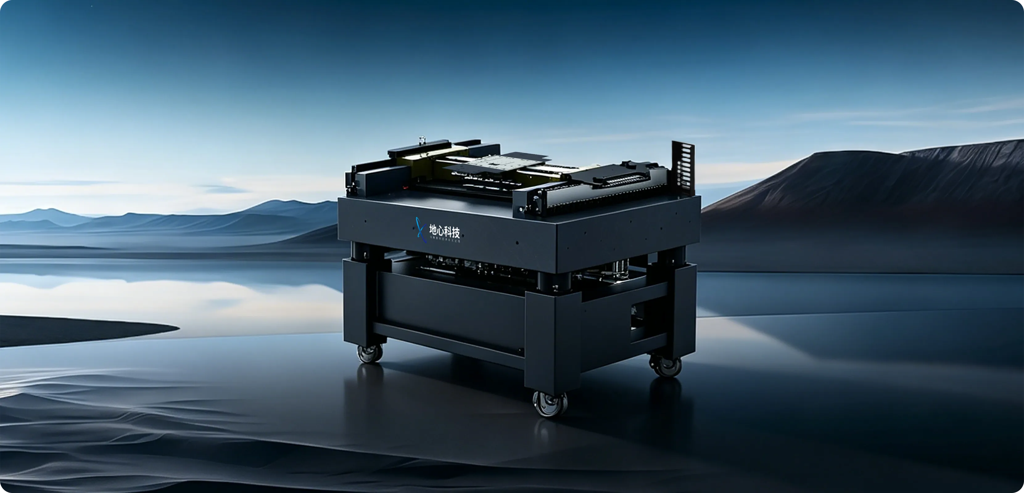
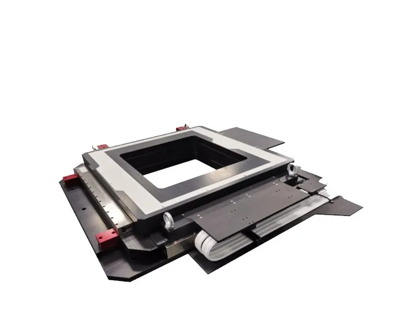
In photomask inspection applications, a backlight source is often required, and the motion stage must deliver extremely high positioning accuracy and speed. Coretech's CFTCA series large-aperture 2D motion stage is exceptionally well-suited for such applications.
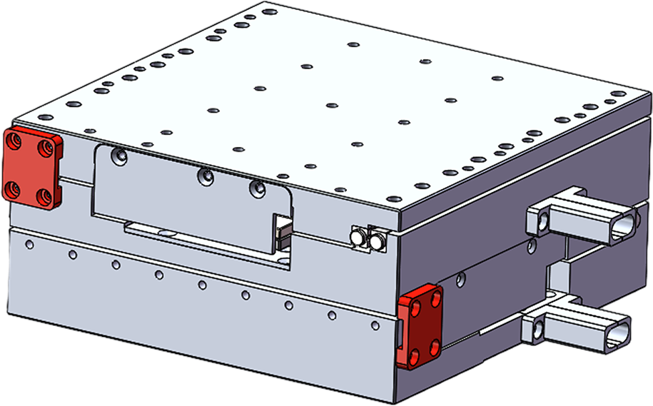
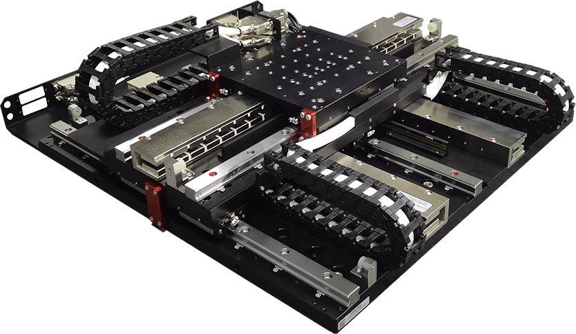
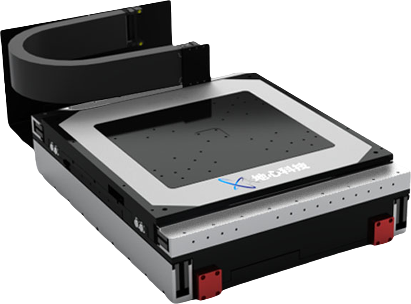
CFTCA Series XY Integrated Precision Positioning Stage with Nanometre-Level Positioning Accuracy
XY integrated direct-drive stage with large aperture, high dynamic performance
Cross-roller guides for compact construction
Low lateral height for reduced Abbe error
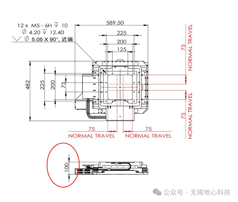
Travel options: 150 mm × 150 mm and 250 mm × 250 mm
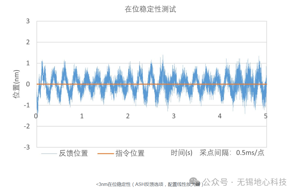
Resolution: 1 nm; repeatability: ±150 nm; positioning accuracy: ±300 nm; in-position stability: 3 nm
| 平台型号\Model | CFTCA-150XY | CFTCA-250XY |
| 有效行程(mm) | 150*150 | 250*250 |
| 中空尺寸(mm) | 200*200 | 310*310 |
| 最小安全中空尺寸(mm) | 40*40 | 50*50 |
| 绝对定位精度\Accuracy | ±0.3 µm | ±0.8 µm |
| 双向重复定位精度\Bi-Repeatability | ±0.15 µm | ±0.4 µm |
| 俯仰\Pitch | 15 arc sec | 20 arc sec |
| 偏摆\Yaw | 10 arc sec | 15 arc sec |
| 正交性\Orthogonality | 15 arc sec | 15 arc sec |
| 直线度\Straightness | ±2 µm | ±4 µm |
| 平面度\Flatness | ±2 µm | ±4 µm |
| 平台重量\Stage Mass | 40kg | 70kg |
| 最大负载\Load Capacity | 20 kg | 40 kg |
04 Test Results
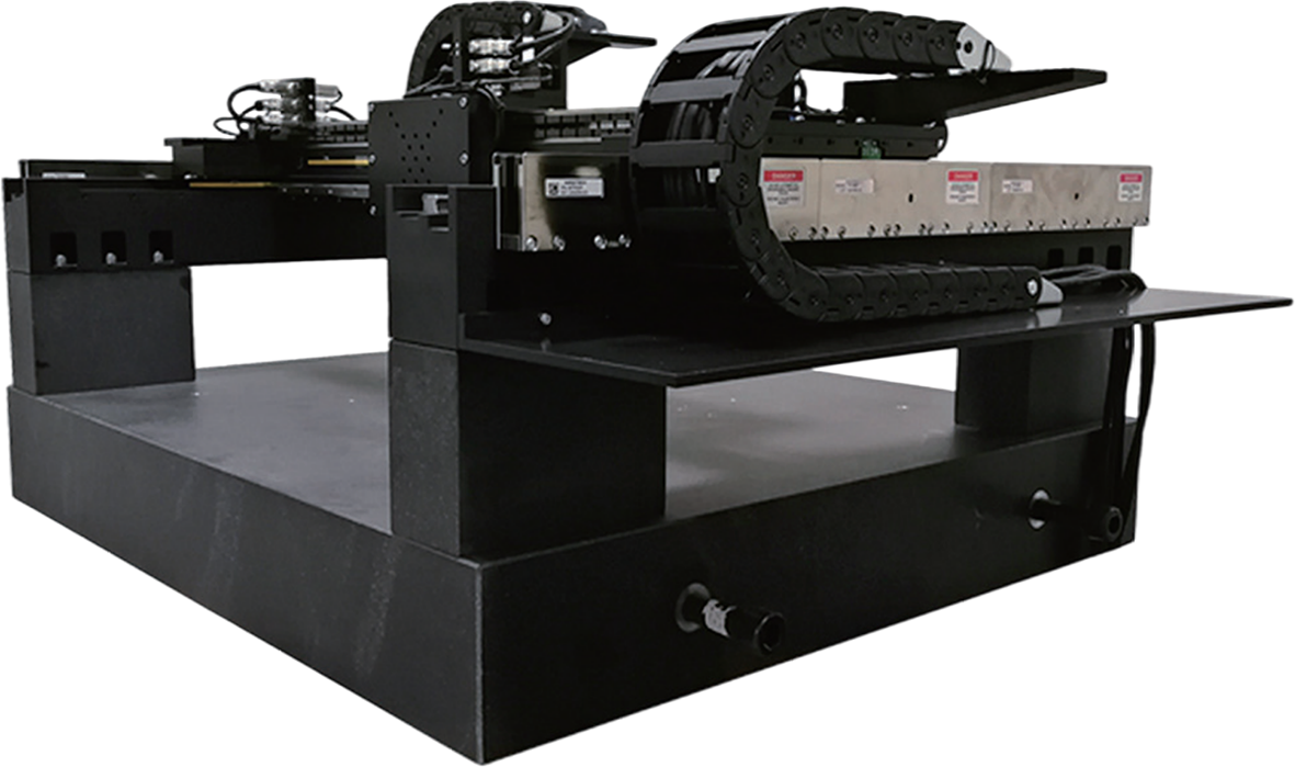
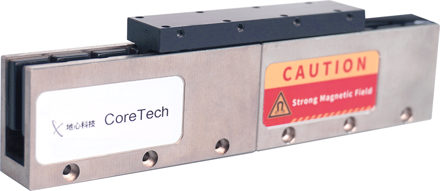
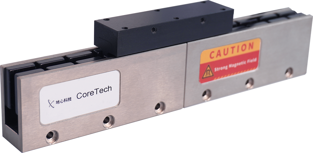
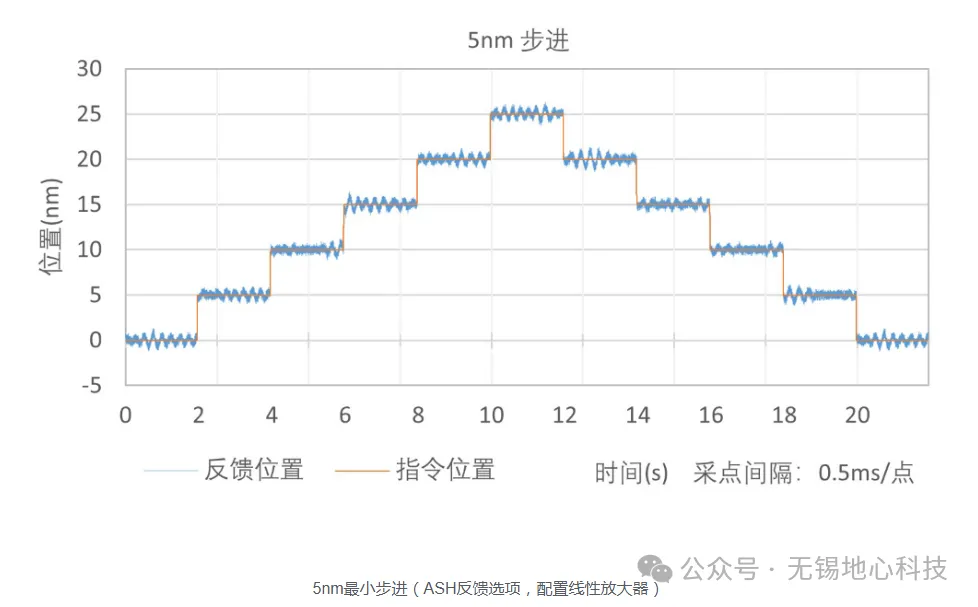
The CFTCA series is driven by linear motors and employs precision cross-roller guides, delivering outstanding dynamic performance and positioning accuracy, with a no-load cutoff frequency exceeding 100 Hz. The CFTCA series features a refined, compact structure yet offers strong driving capability: the upper axis achieves a maximum speed of 1000 mm/s and a no-load acceleration of up to 1 g. Configured with a linear amplifier in a vibration-isolated laboratory environment, the CFTCA series large-aperture stage achieves in-position stability of 3 nm and a minimum step of less than 5 nm. Owing to its large aperture design, it is ideally suited for double-sided measurement and inspection, biological sample processing and observation, thin-film thickness measurement, and other industrial and research applications that demand nanometre-level positioning accuracy and a large central opening.
Featured News
Laser Processing Automation Solutions – PCB Drilling
2026.06.03
High-Precision Motion Stages Enhancing Coupling Alignment Accuracy in Precision Fiber Coupling Equipment
2026.06.03
Breaking the Boundaries of Chip Yield Improvement: Geocentric Technology's Wafer Spiral Inspection Solution Accelerates Quality and Efficiency in the Industry
2026.06.03
 Back to List