
.png)

.png)







Home
 News Center
One Article Summary | Multiple Applications of Precision Motion Stages in Wafer Defect Inspection
News Center
One Article Summary | Multiple Applications of Precision Motion Stages in Wafer Defect Inspection
News Center
One Article Summary | Multiple Applications of Precision Motion Stages in Wafer Defect Inspection
One Article Summary | Multiple Applications of Precision Motion Stages in Wafer Defect Inspection
 2026-06-03
Share:


Semiconductor manufacturing involves complex processes; to ensure quality, nearly every process step requires rigorous inspection. If defective dies proceed to subsequent stages, they not only severely compromise the overall product quality but also lead to significant increases in production costs. In this context, whether in automated optical inspection (AOI) systems or scanning electron microscope (SEM) systems, the precision motion stage that carries the wafer is the core component determining inspection accuracy and efficiency.
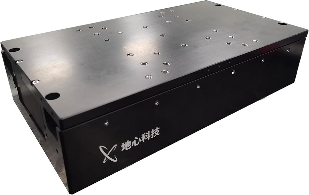
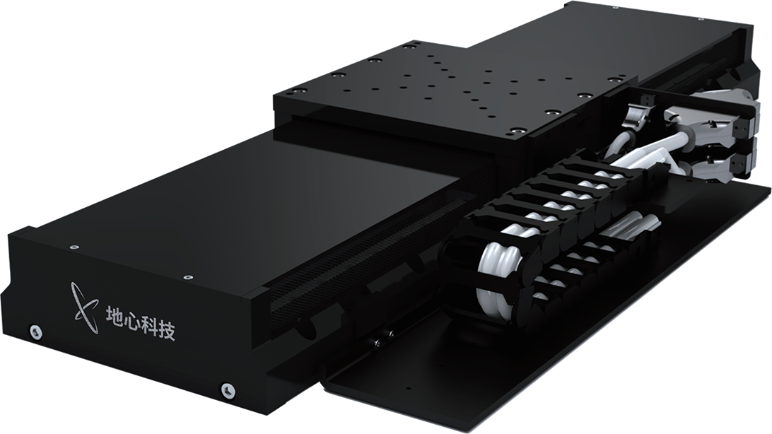
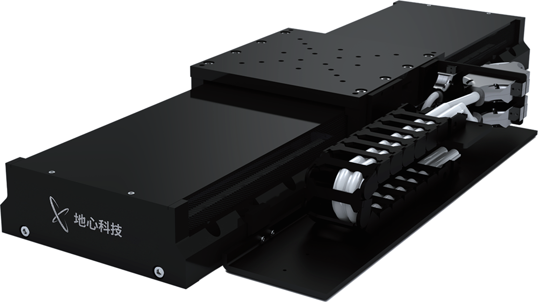
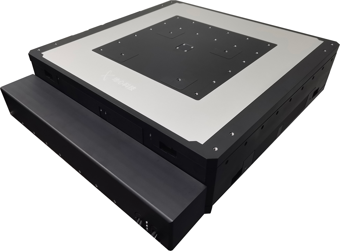
Addressing the requirements for wafer surface defect and dimension inspection, the various series of motion stages from Geocentric Technology can provide diversified performance solutions for automated inspection equipment integrators. They support multiple modes, including serpentine reciprocating on‑the‑fly linear scanning, area‑scan camera point‑to‑point region inspection, and high‑speed spiral trajectory inspection, enabling accurate and efficient wafer screening.
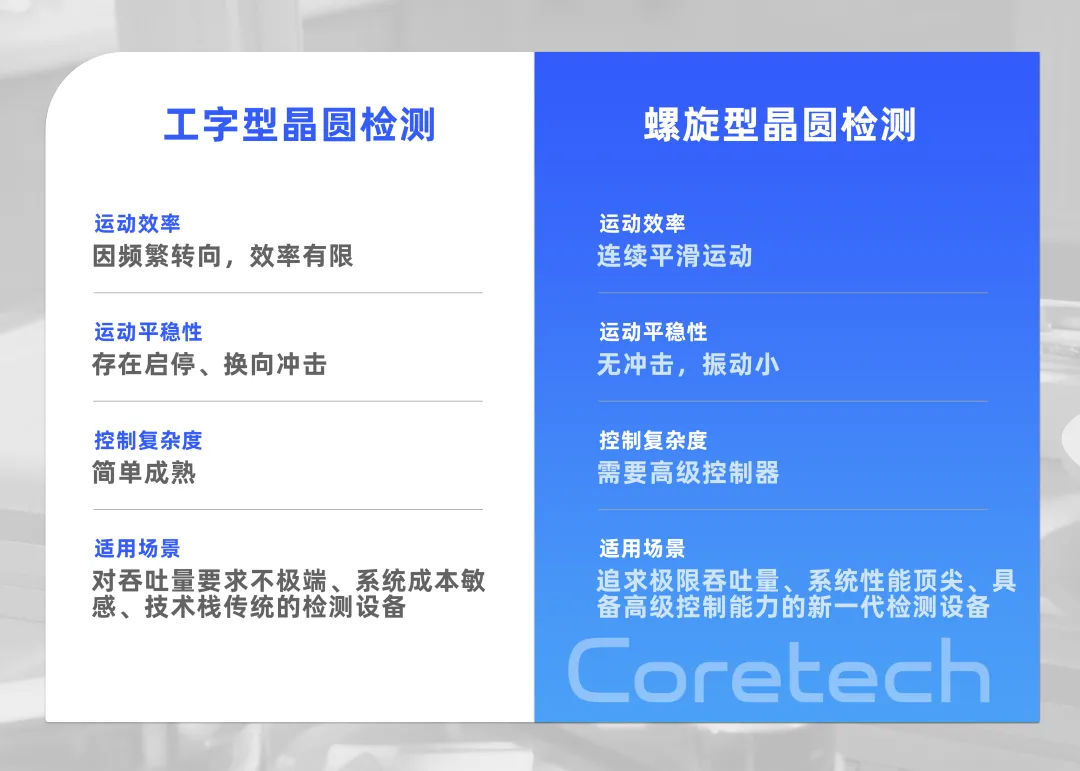
Comparison of characteristics between raster‑type and spiral‑type wafer inspection
01 Raster‑Type Wafer Defect Inspection
Raster scanning, also known as grid scanning, is one of the most widely adopted path‑planning methods in wafer inspection. The motion stage performs continuous reciprocating scans along the X‑axis; after completing each row, the Y‑axis steps by a fixed distance, and the process repeats, forming a path resembling the character "工" (or a raster pattern).
This inspection method features a simple and clear path plan, straightforward motion control logic, and relatively modest demands on the controller. The algorithms for image stitching and data correlation are also mature and stable. Meanwhile, the acquired image data is arranged in a row‑column matrix format, facilitating storage, localization, and traceability of defect positions.
Geocentric Technology has extensive experience in the custom development of raster‑scan motion stages and can perform targeted optimisations based on specific customer application requirements, ensuring seamless adaptation to production line processes.
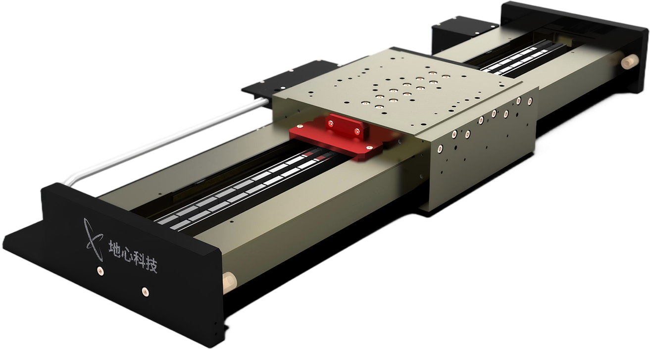
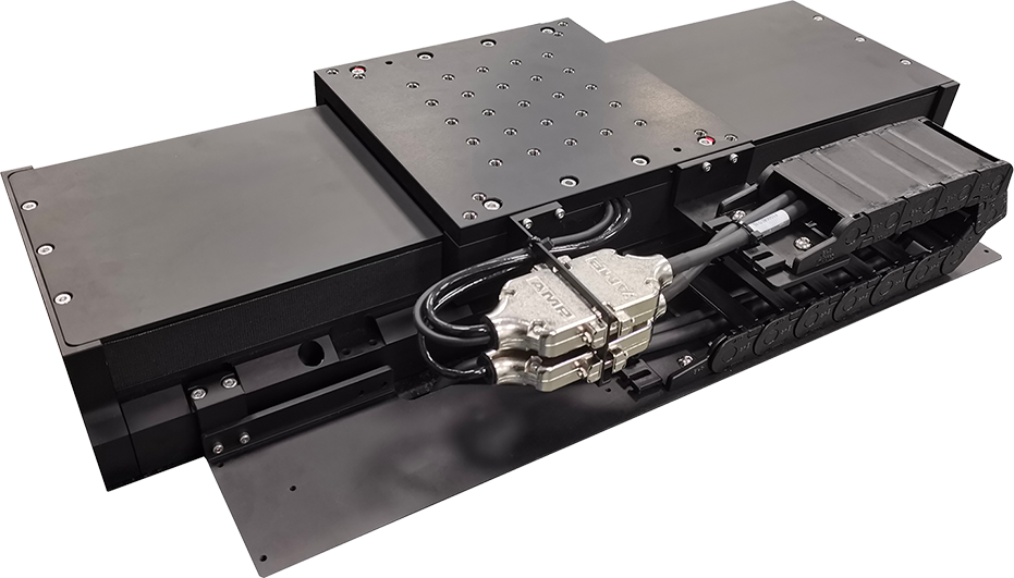
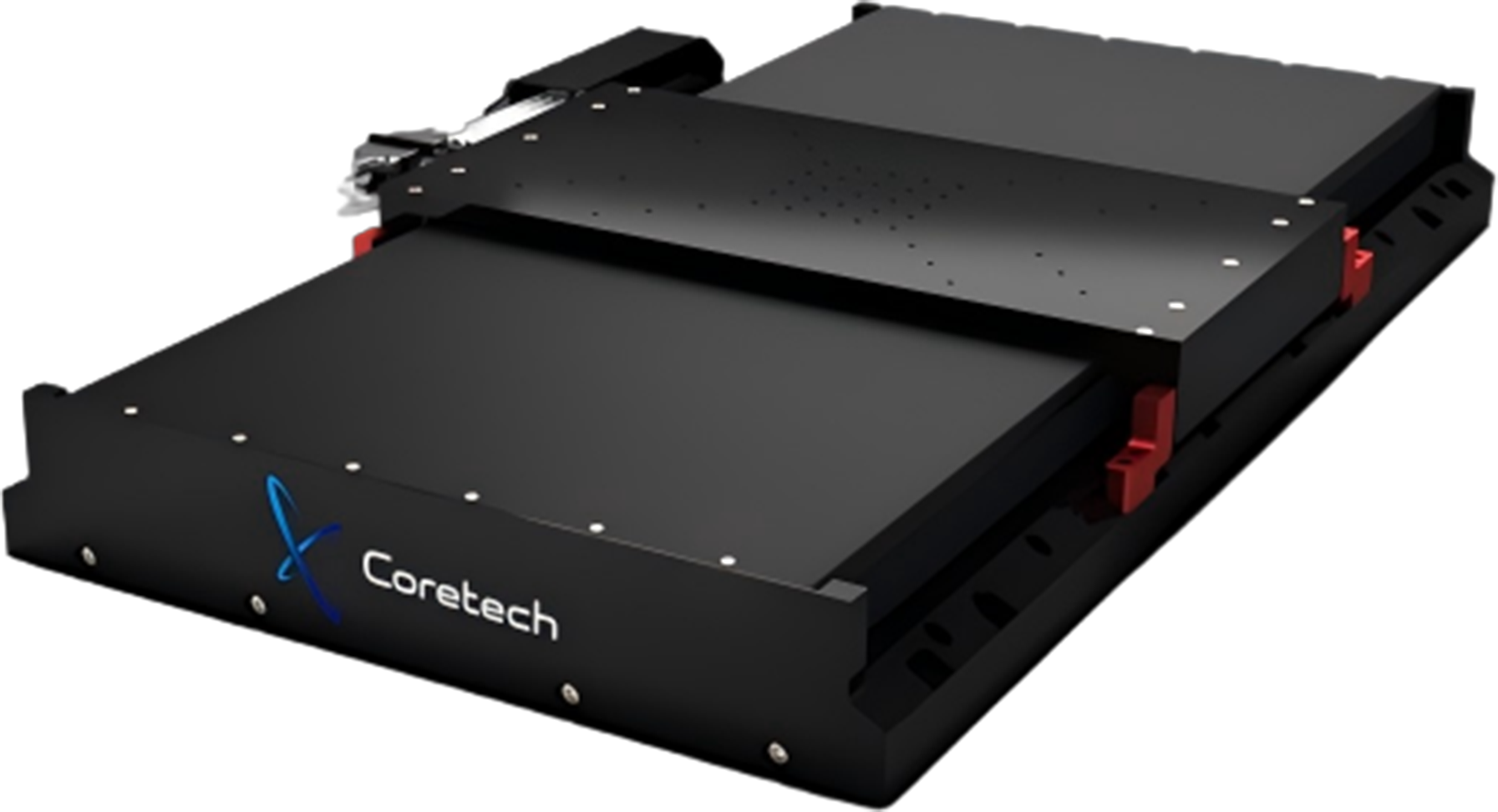
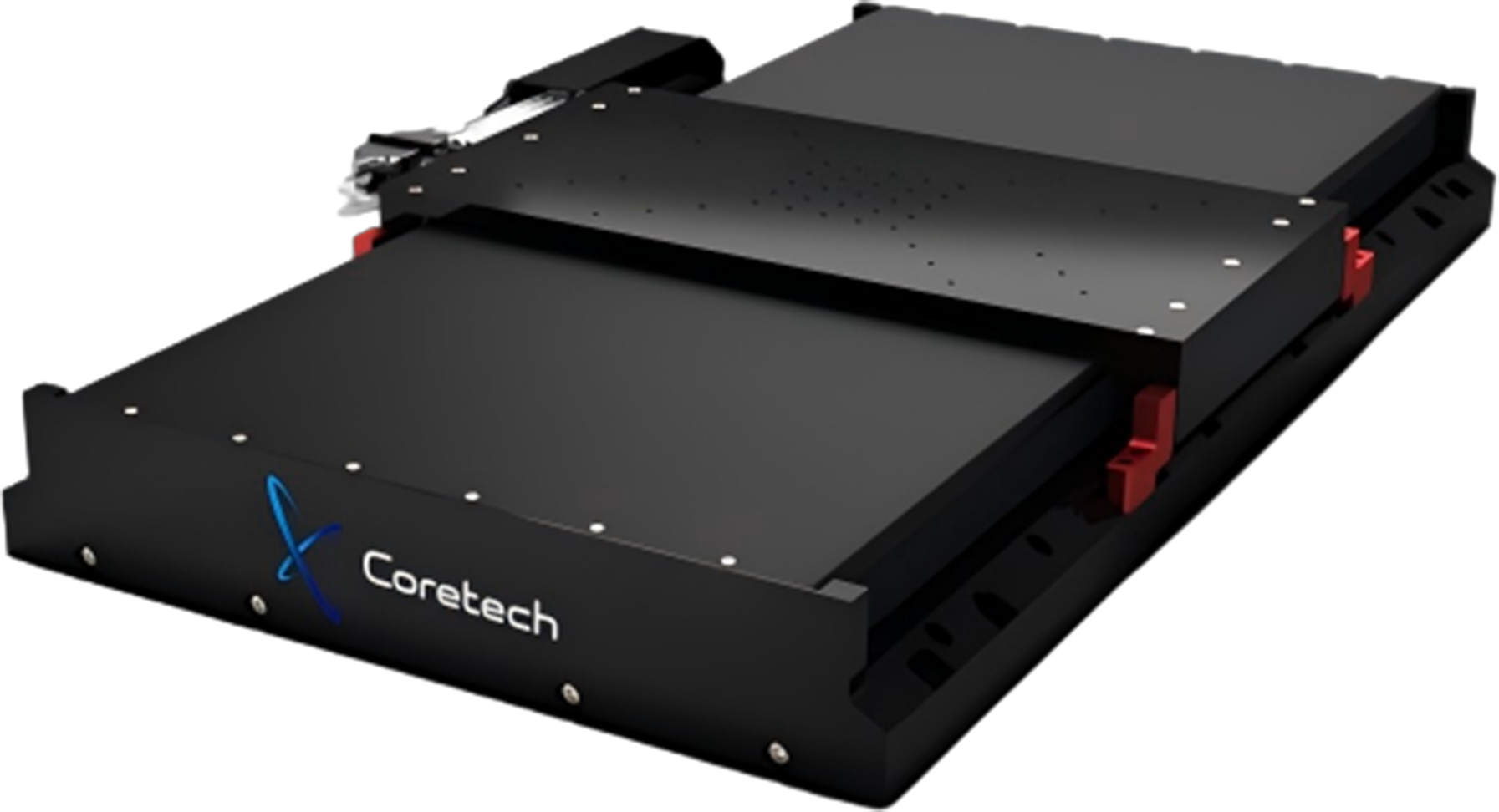
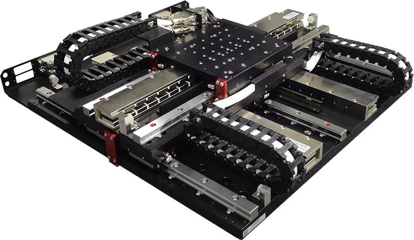
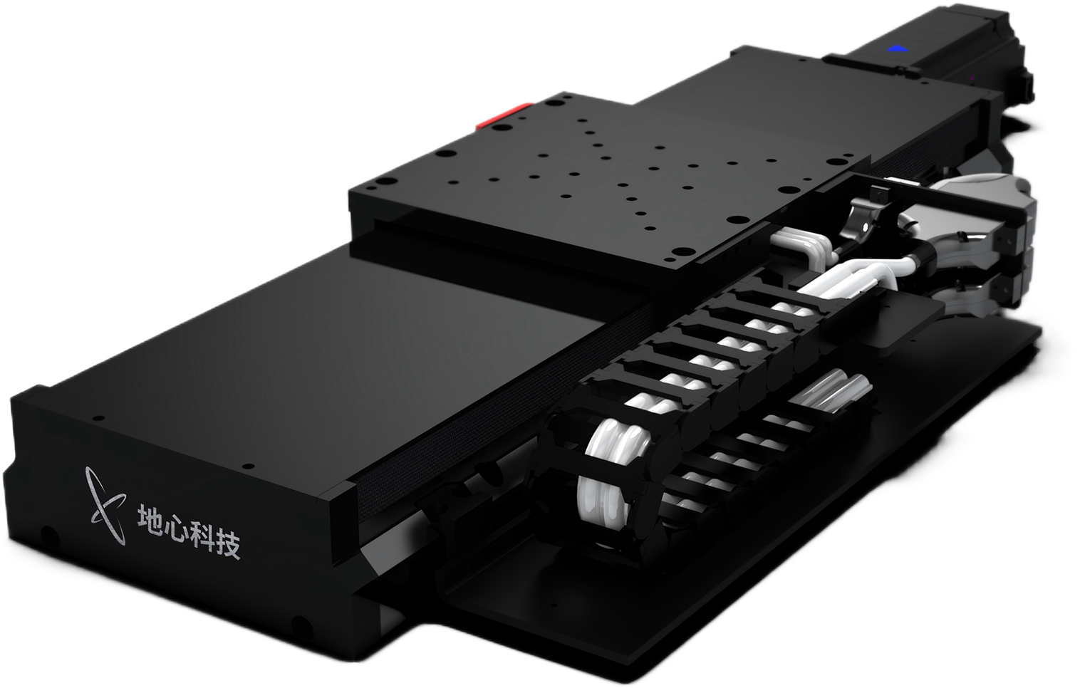
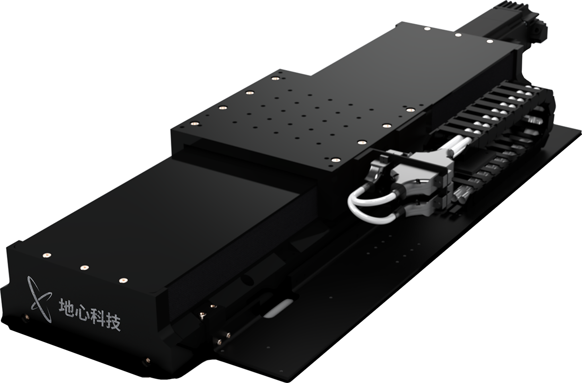
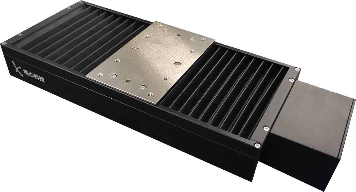
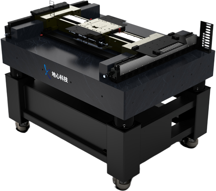
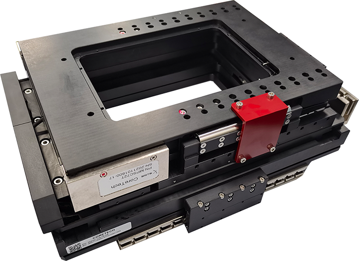
OneXY Linear Stage + ART165V‑5 Z‑Lift Stage
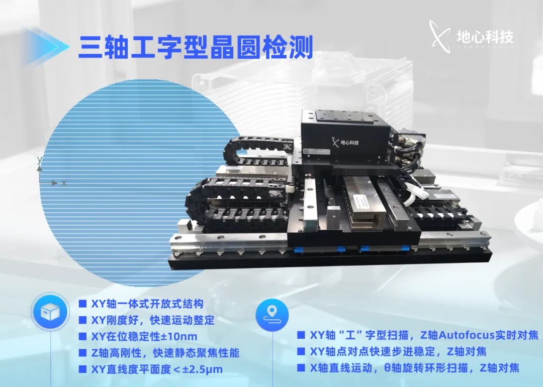
Function: Fast step‑and‑settle
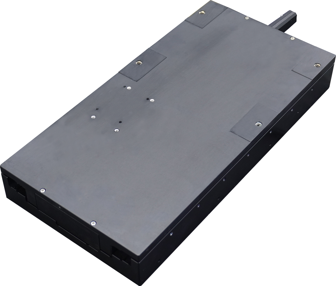
Product: OneXY‑350‑350
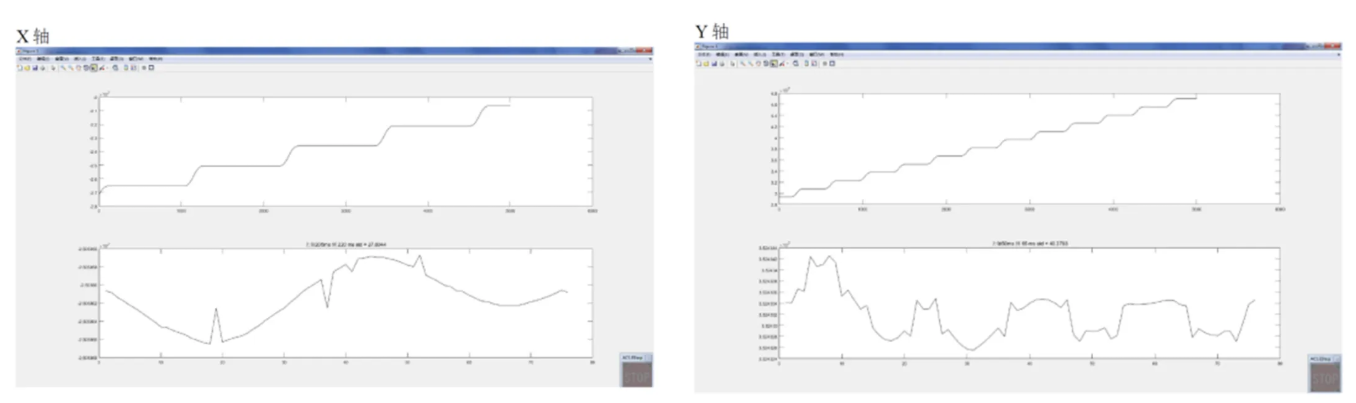
Specifications:
Y‑axis step: 1.47 mm (IMA10T exposure field width), motion time 50 ms, settling window 50 nm
X‑axis step: 1.47 mm (IMA10T exposure field width), settling time 205 ms, settling window 50 nm
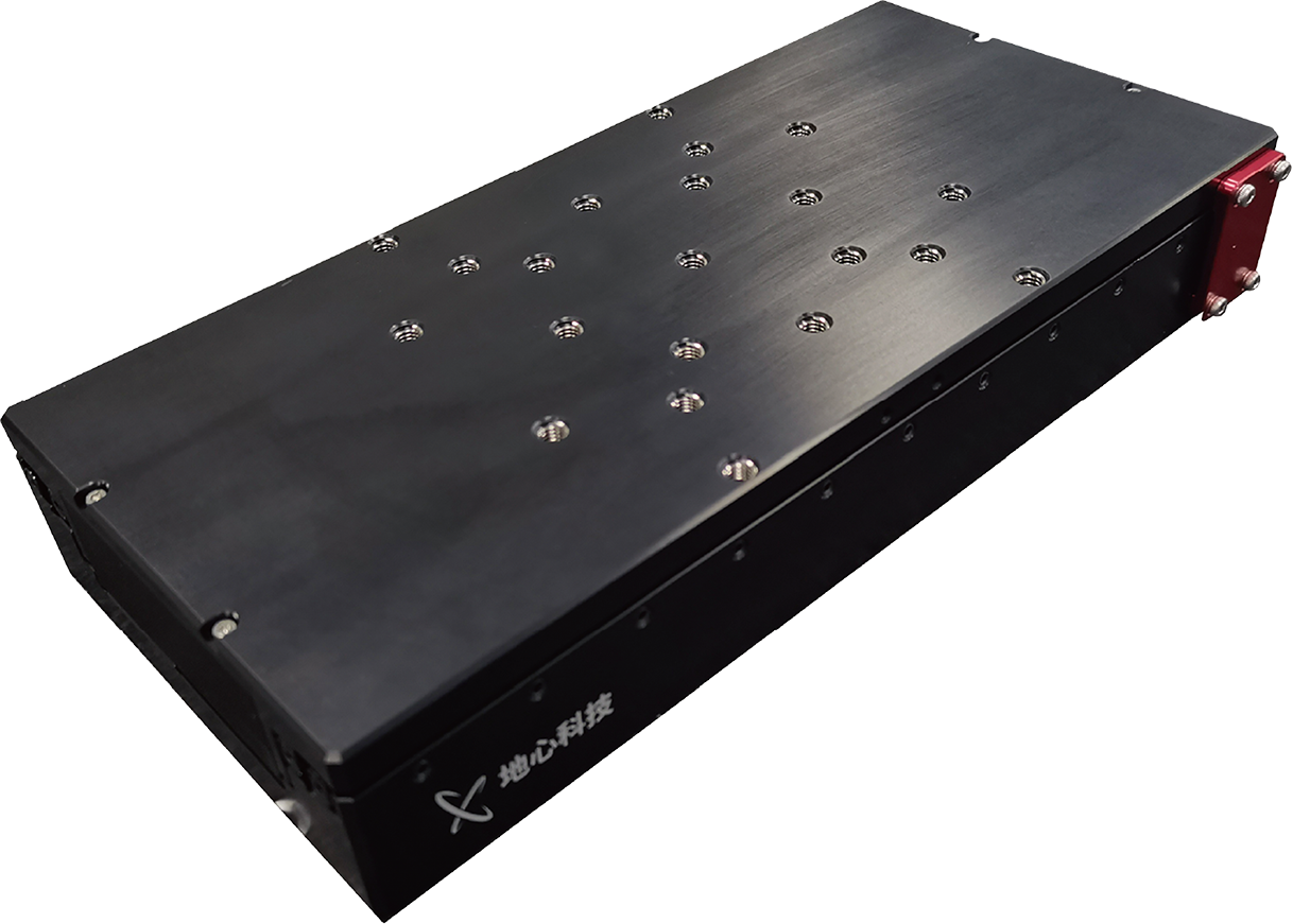
Surface Air Bearing+Surface Z+Surface T
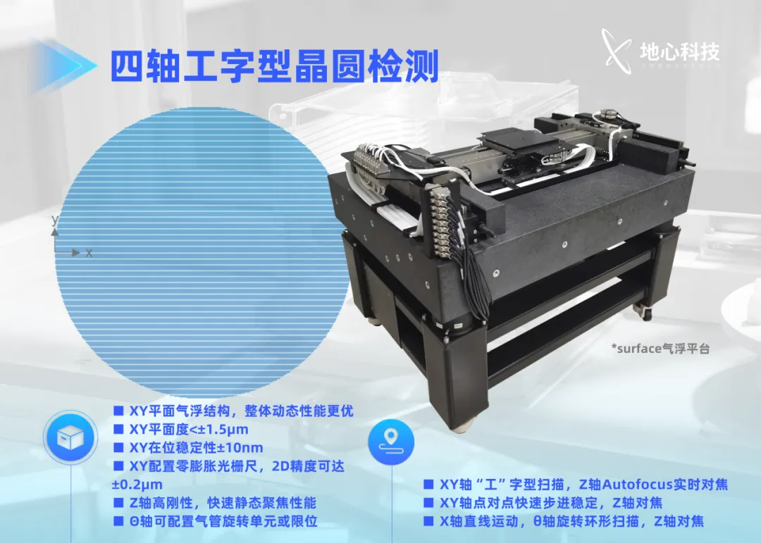
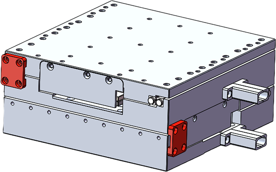
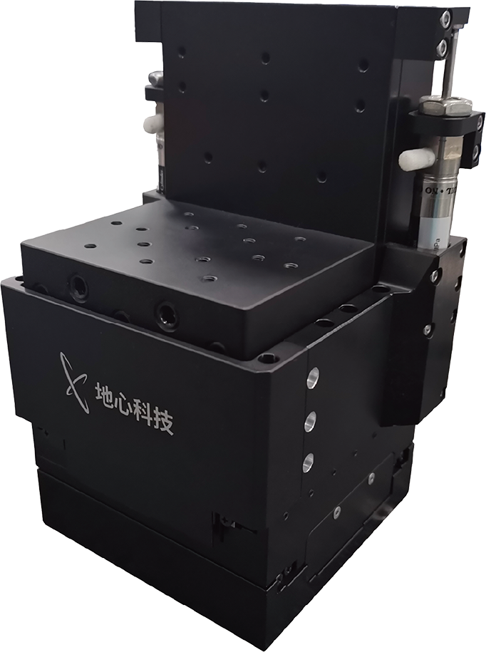
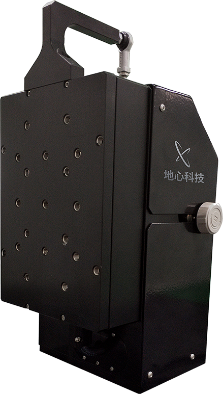
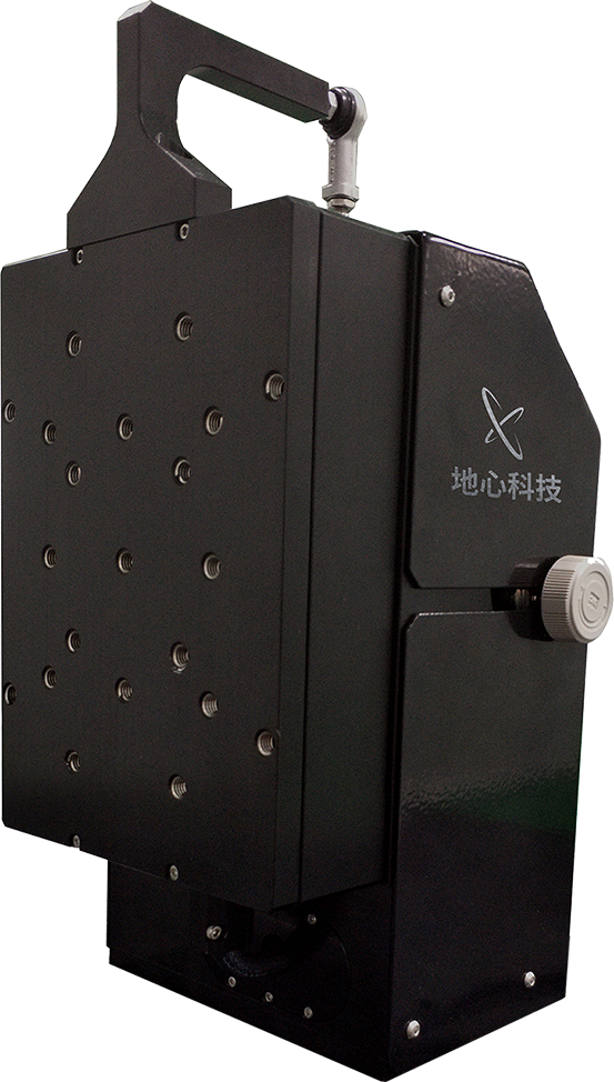
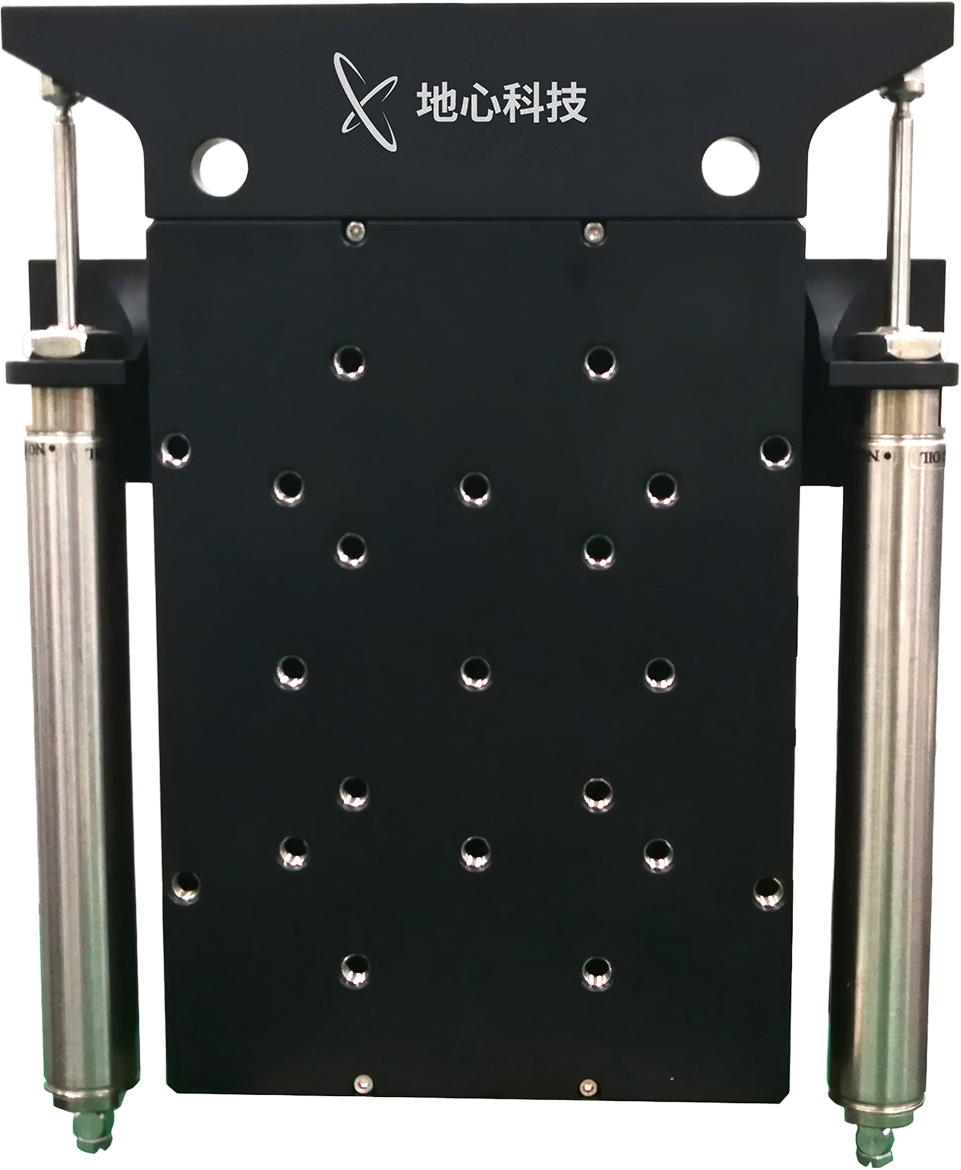
Surface‑Z Series Direct‑Drive Z‑Lift Stage – Auto‑Focus
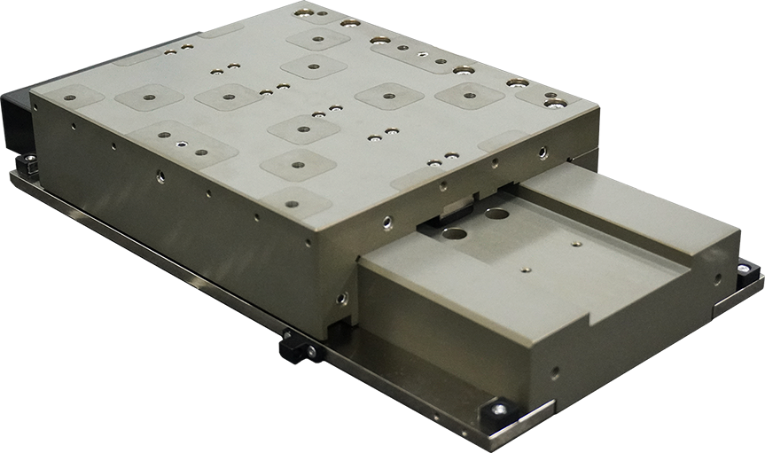
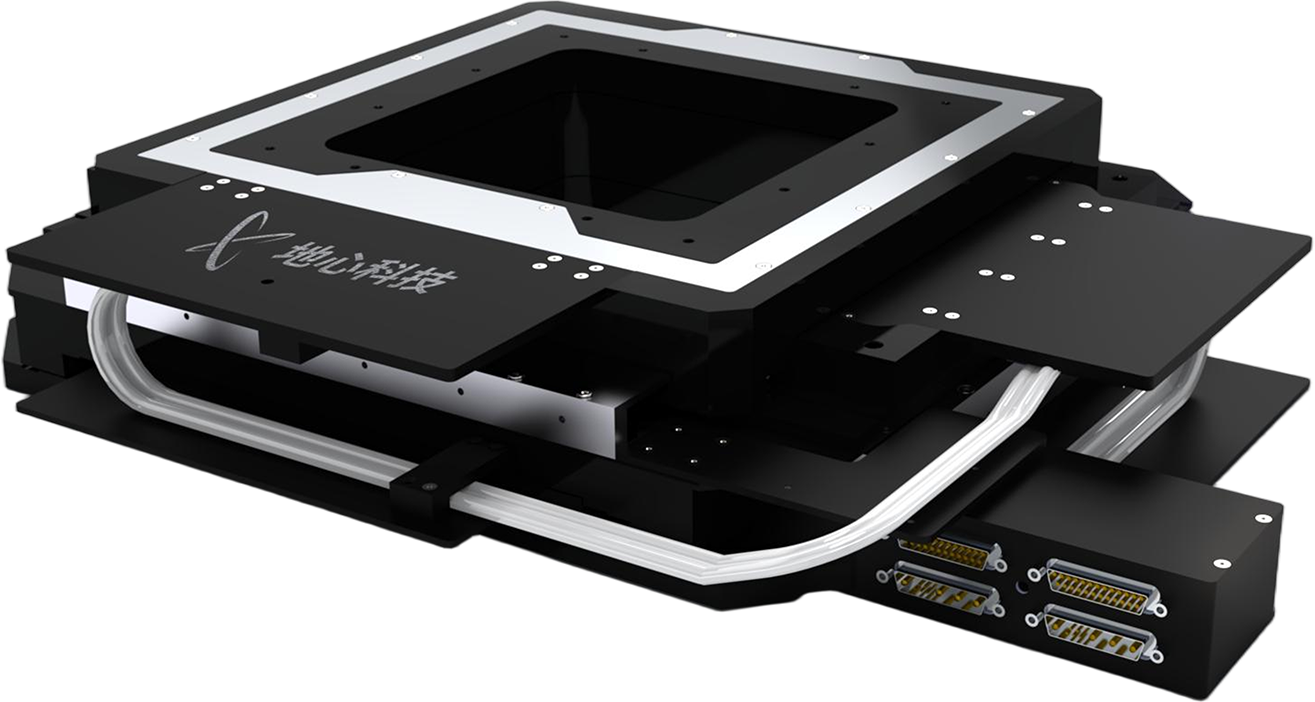
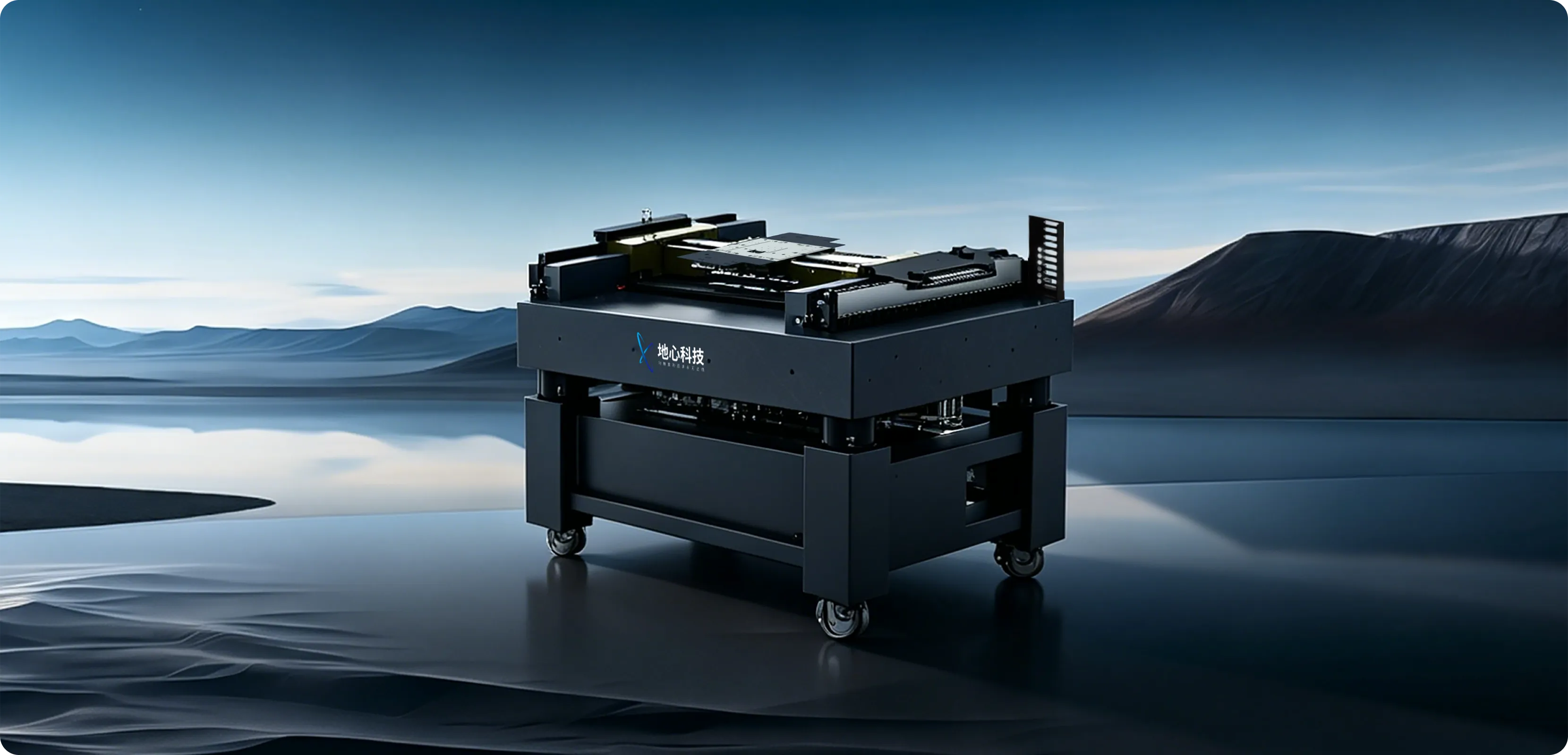
To address the auto‑focus challenges caused by wafer surface non‑flatness or warpage, Geocentric Technology offers a classic solution: an open‑frame platform with an integrated XY design (ONEXY‑350‑350), paired with a high‑precision Surface Z lift stage. The X‑axis performs step motions, the Y‑axis executes the raster scanning, and the Z‑lift stage compensates for wafer height fluctuations in real time, ensuring that the surface under inspection remains within the optimal depth of focus of the camera.
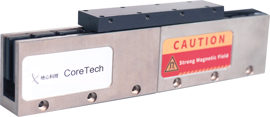
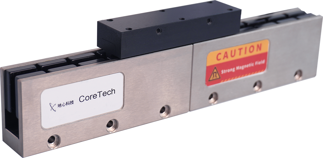
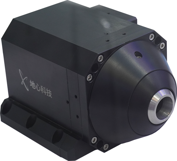
As a vertical motion platform designed specifically for precision positioning, the Surface Z employs a linear motor drive and cross‑roller guide structure, achieving nanometre‑level positioning accuracy and excellent dynamic performance. With a no‑load closed‑loop cutoff frequency exceeding 200 Hz, it offers rapid response, stability, and reliability.
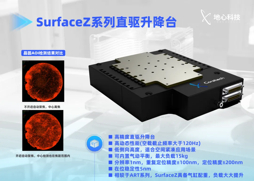
Function: Auto‑focus
Product: Surface Z‑5 (suitable for 8‑inch to 12‑inch wafers)
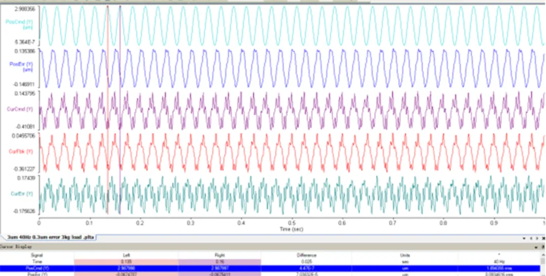
Performance: 3 μm amplitude, 40 Hz @ ±150 nm dynamic following error
Features: Direct‑drive motor / Optional built‑in zero‑friction air cylinder for load balancing
02 Spiral‑Type Wafer Defect Inspection
Compared with traditional raster scanning, spiral‑type wafer inspection paths are more suitable for advanced process nodes and high‑efficiency production lines. The inherent continuous‑path characteristic of spiral motion enables full‑wafer coverage in a single scan, reducing mechanical movement time by approximately 40% compared with conventional raster movement.
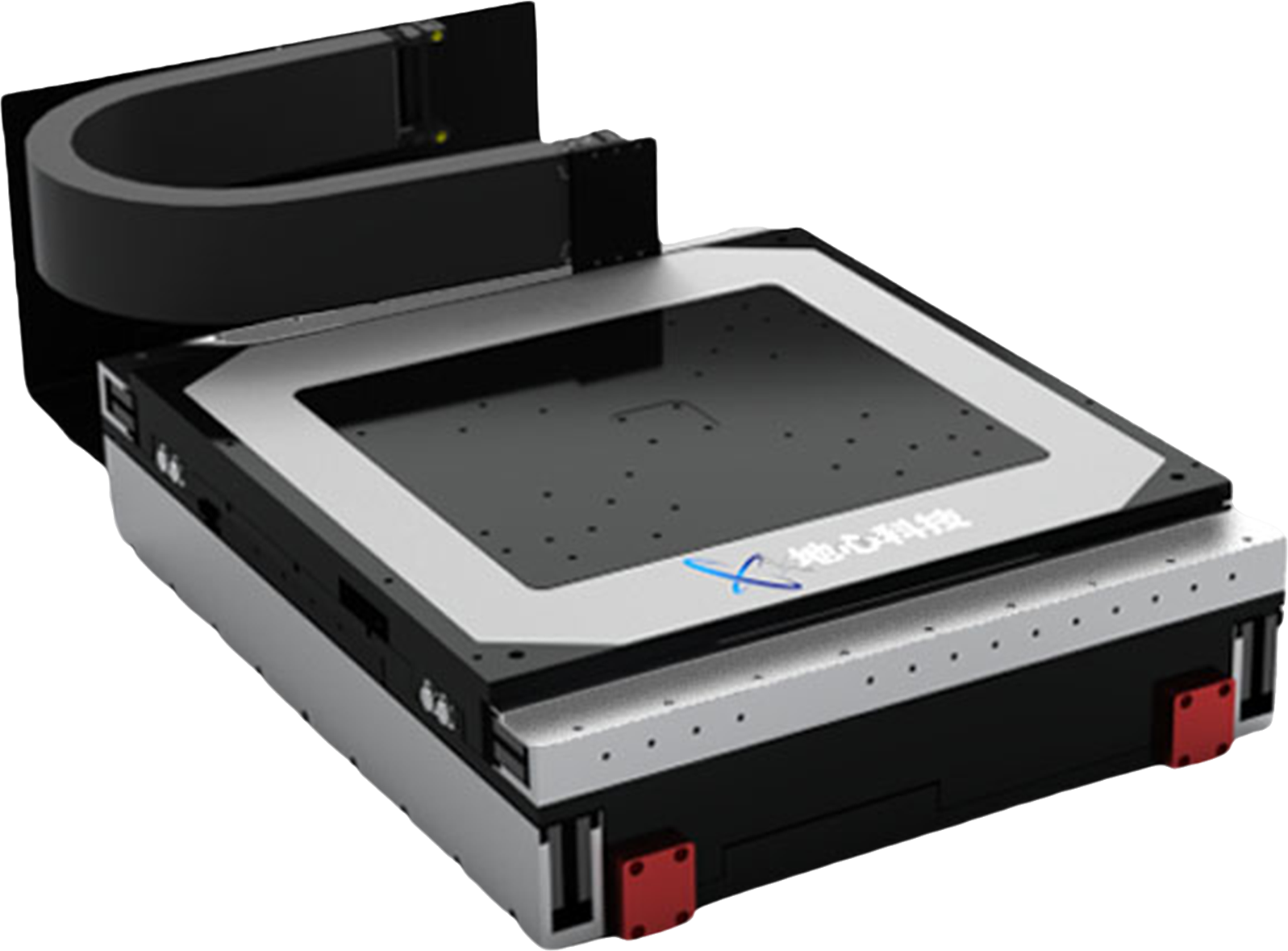
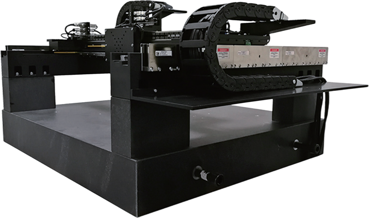
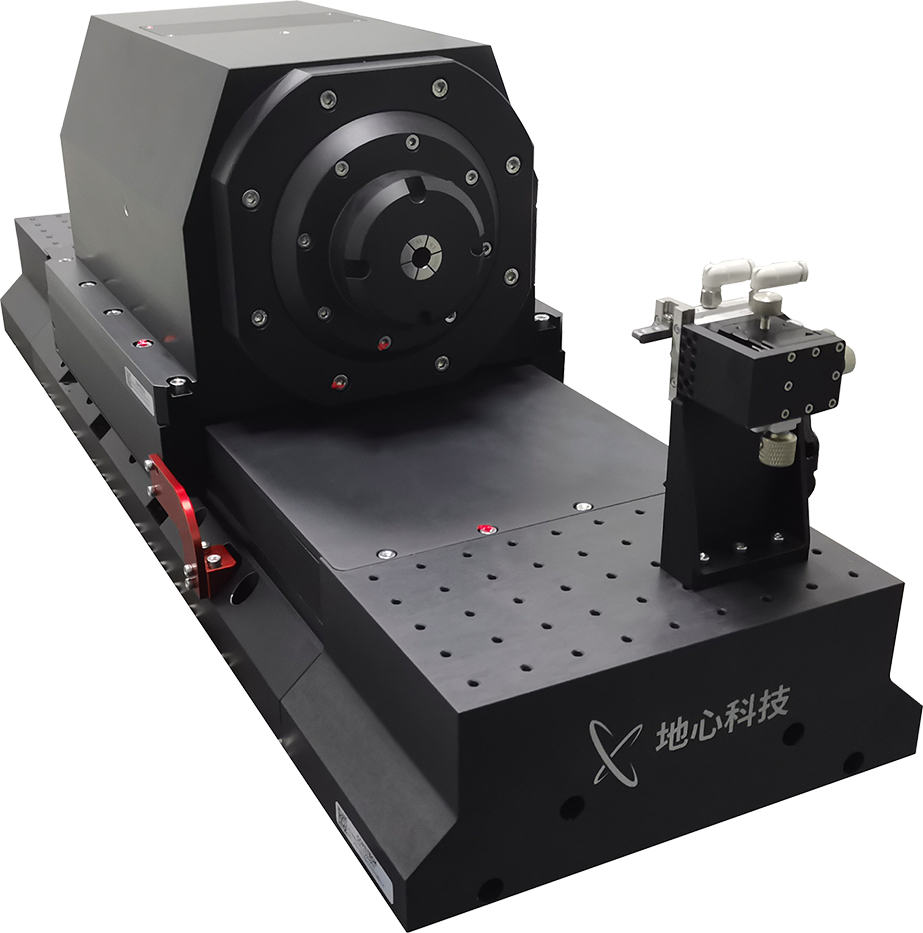
Wuxi Geocentric Technology offers customised spiral inspection solutions centred on ultra‑high‑speed air‑bearing rotary stages. Under coordinated operation of linear axes and the rotary stage, the wafer surface motion flatness can be maintained at <5 μm. Together with a Z‑lift stage featuring high dynamic response, precise focusing can be achieved during high‑speed motion. With the rotary stage carrying the chuck at speeds up to 6000 rpm, the disturbance to the linear axes can be controlled within ±0.5 μm, providing a stable imaging foundation for image sensors with higher resolution and smaller pixel sizes.
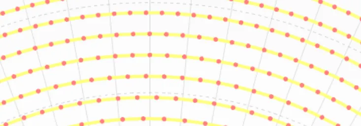
To lower the entry barrier for users, we have developed a dedicated spiral‑path tool software. With simple settings, the motion mechanism can generate the movement path and automatically produce the corresponding trigger points as required. In addition, we provide a dynamic link library (DLL), enabling users to conveniently integrate the entire system into their own measurement systems for efficient and flexible secondary development.
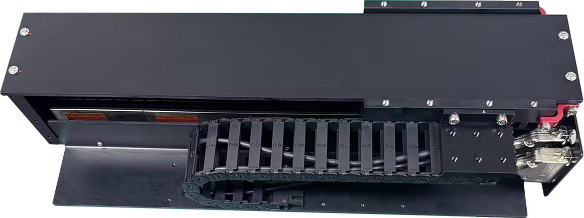
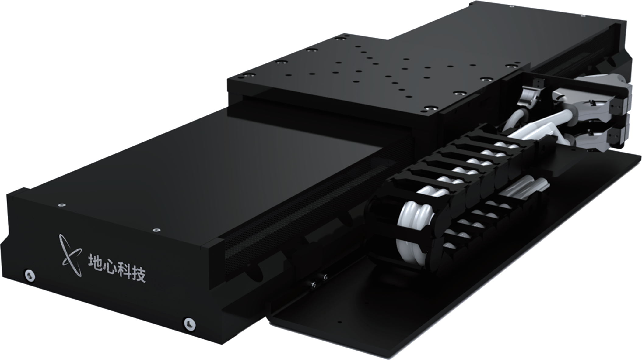
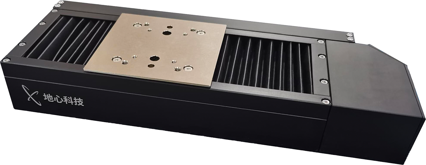
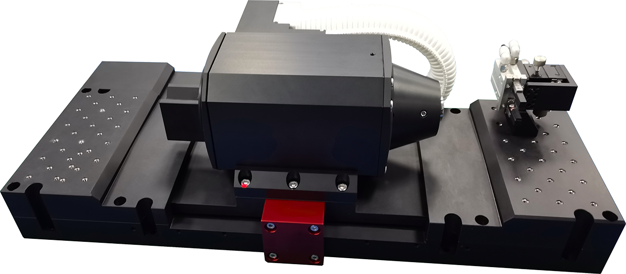
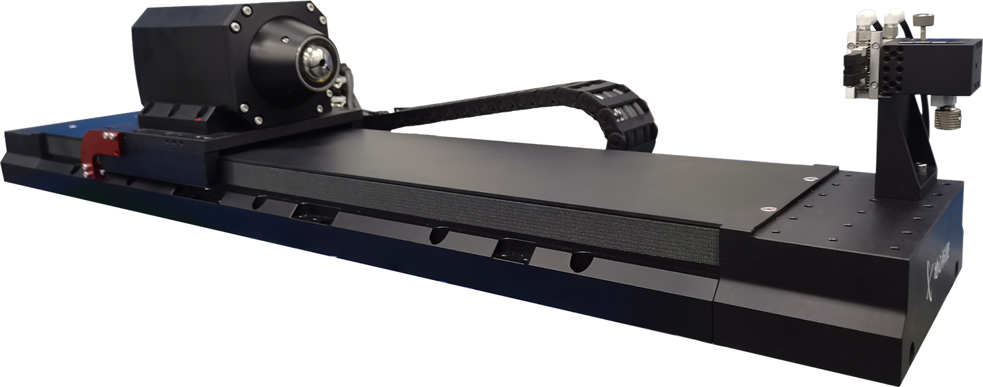
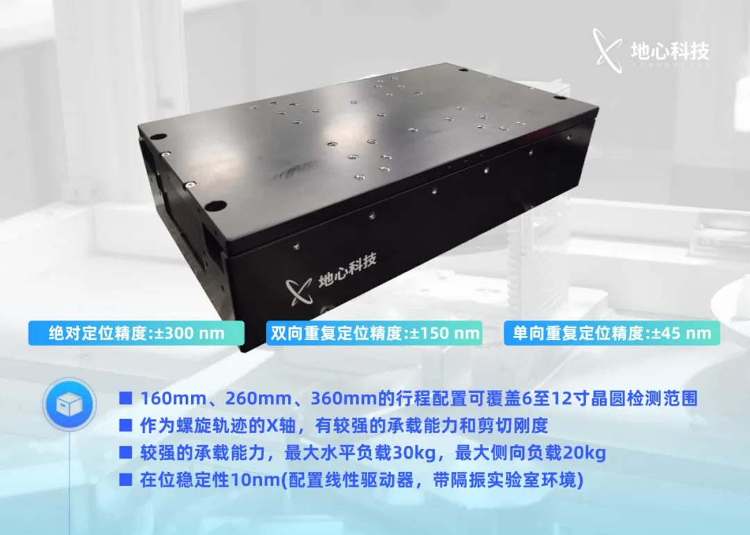
ART180 Linear Stage + SMH165SD + ASP150
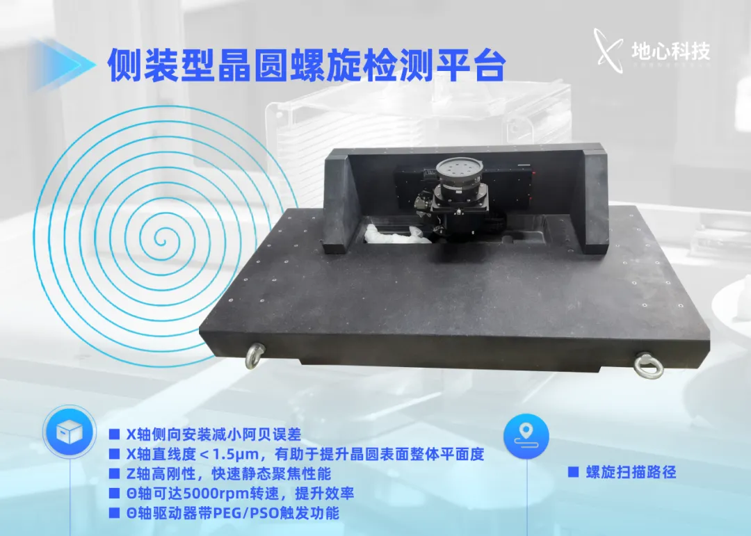
Air‑bearing guides + cross‑roller guides + ASP150
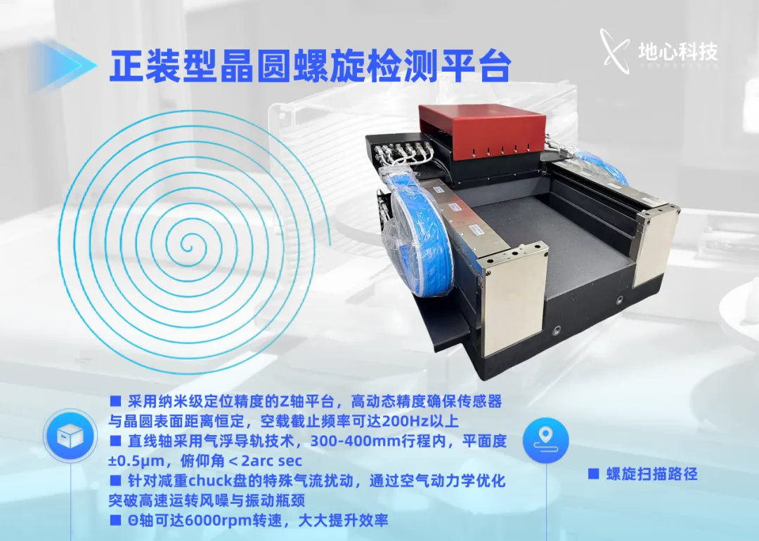
Key Motion Stages for Spiral Inspection
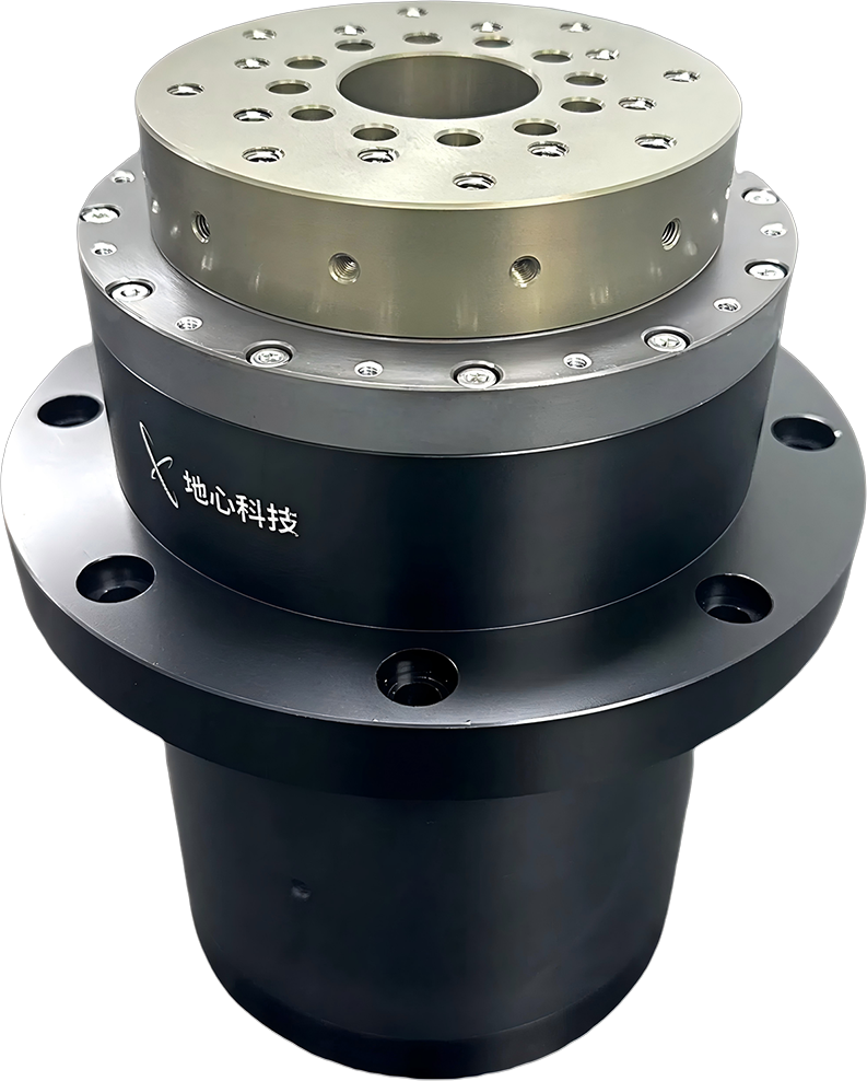
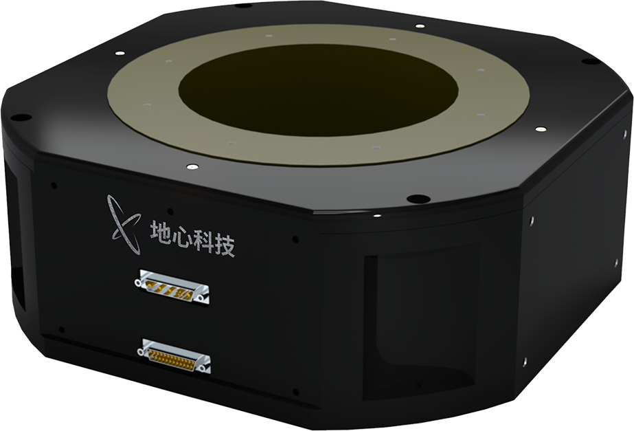
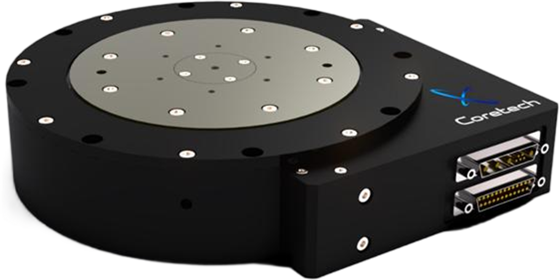
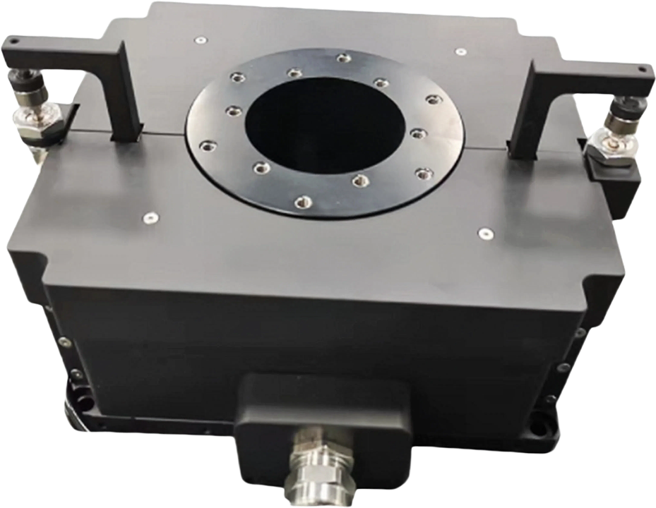
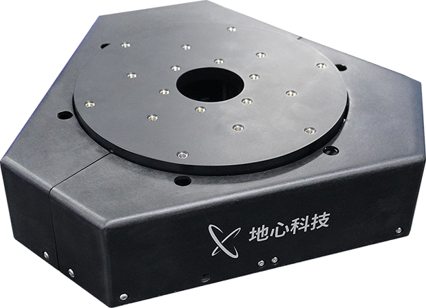
ASP Series Air‑Bearing Rotary Stages
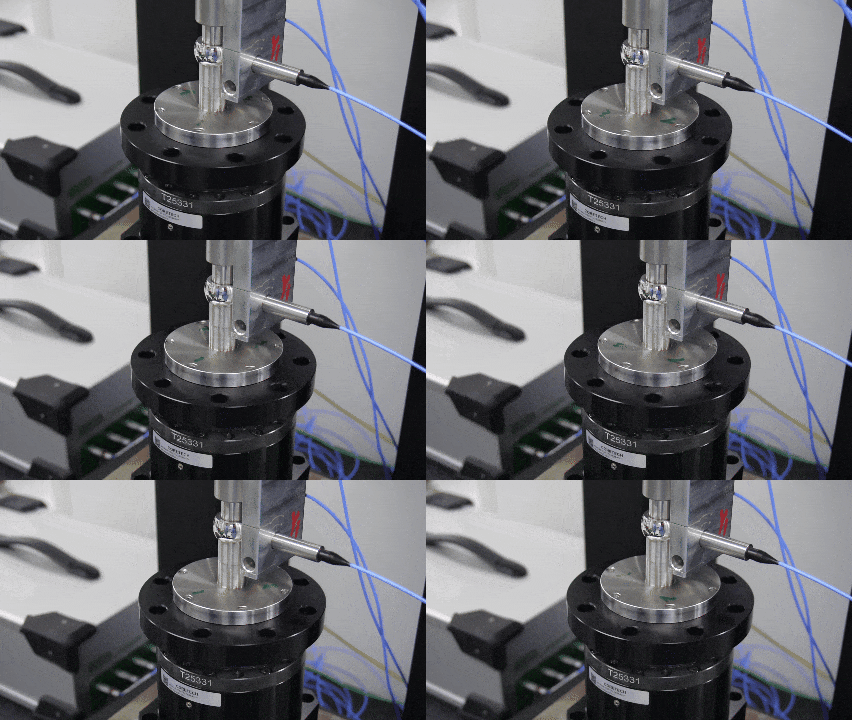
RAB Series Air‑Bearing Rotary Stages
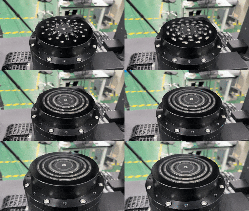
Minimise axial, radial, and tilt error motions
Excellent positioning performance, velocity stability, and high‑resolution feedback
Non‑contact air bearings contribute to ultra‑precise motion performance
Sub‑arc‑second positioning accuracy
Axial and radial runout <250 nm
Optional rotary unions and tubing available based on application needs
Maximum rotational speed: 1500 rpm
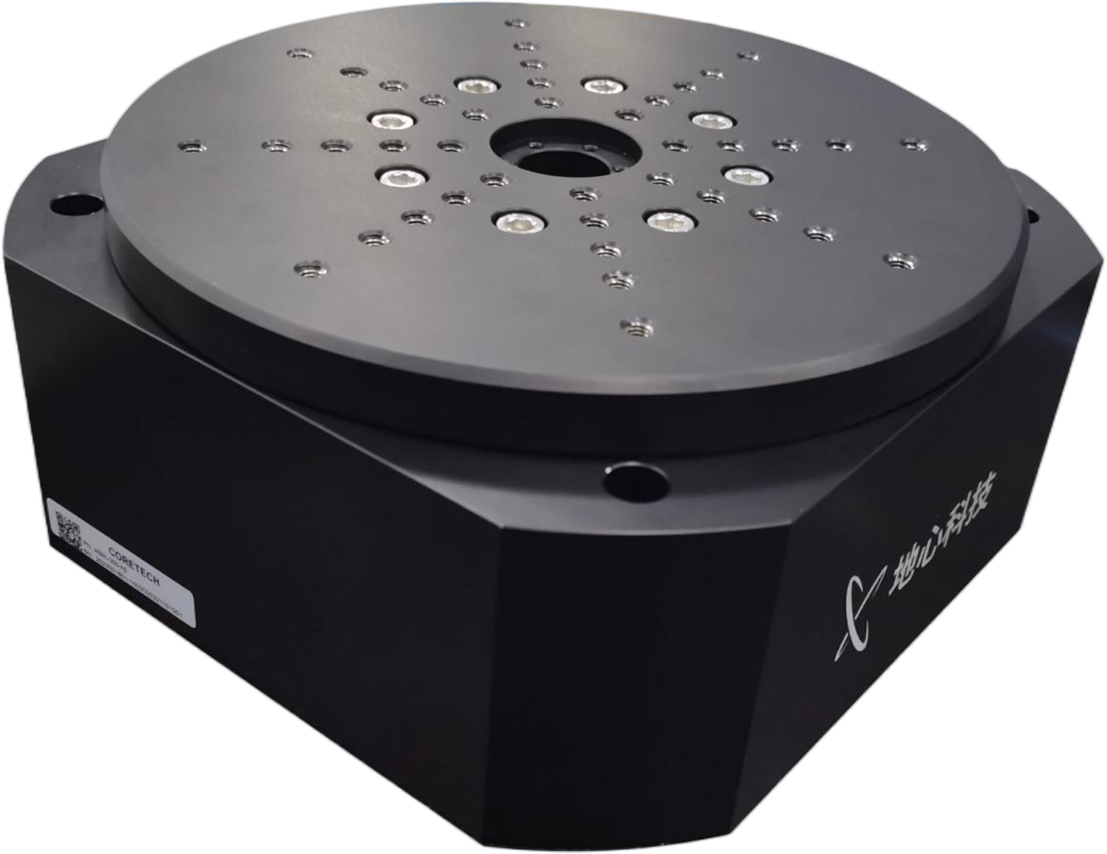
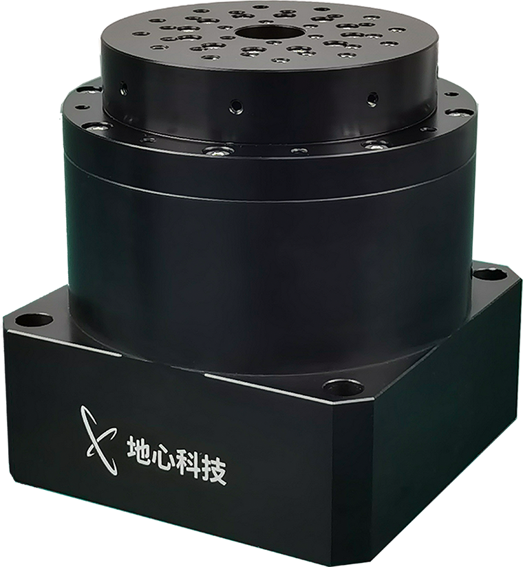
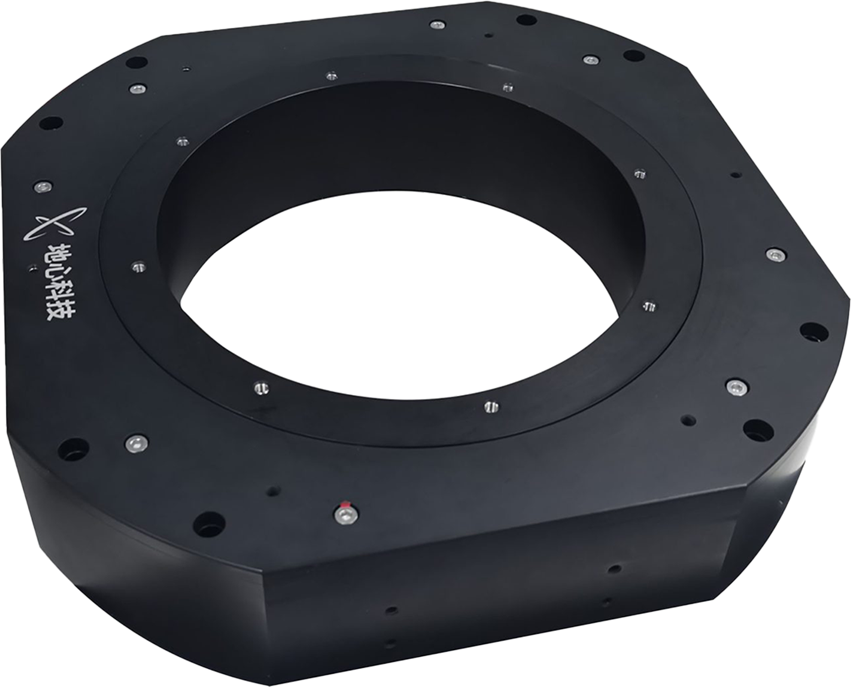
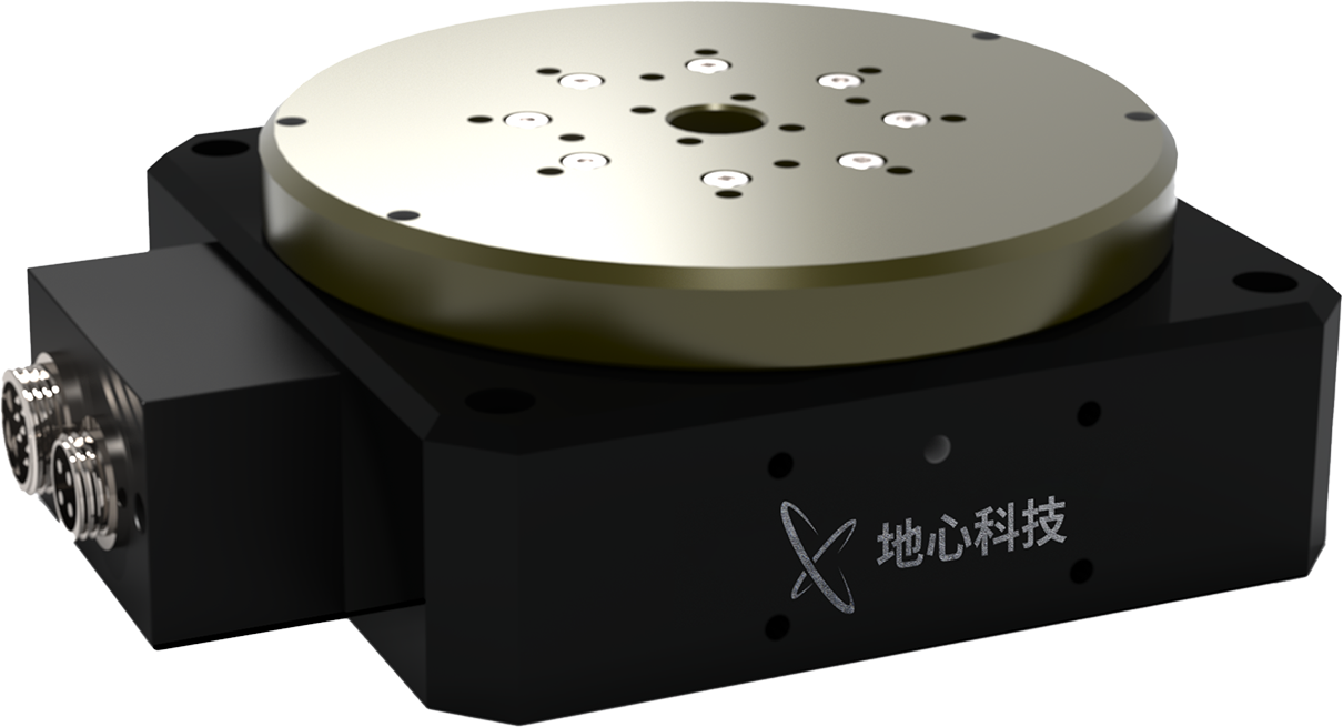
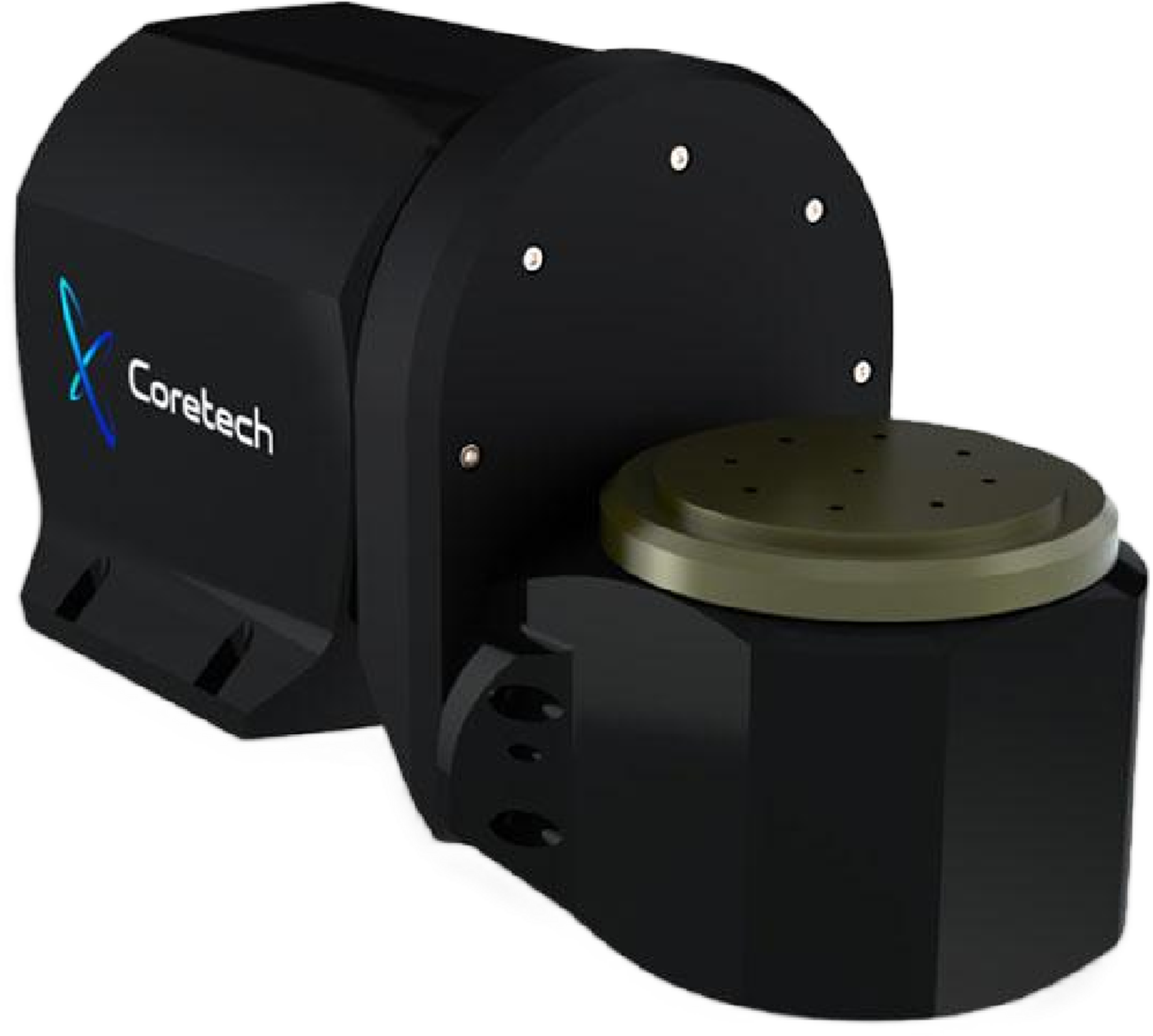
Surface‑Theta Series Mechanical Direct‑Drive Rotary Stages
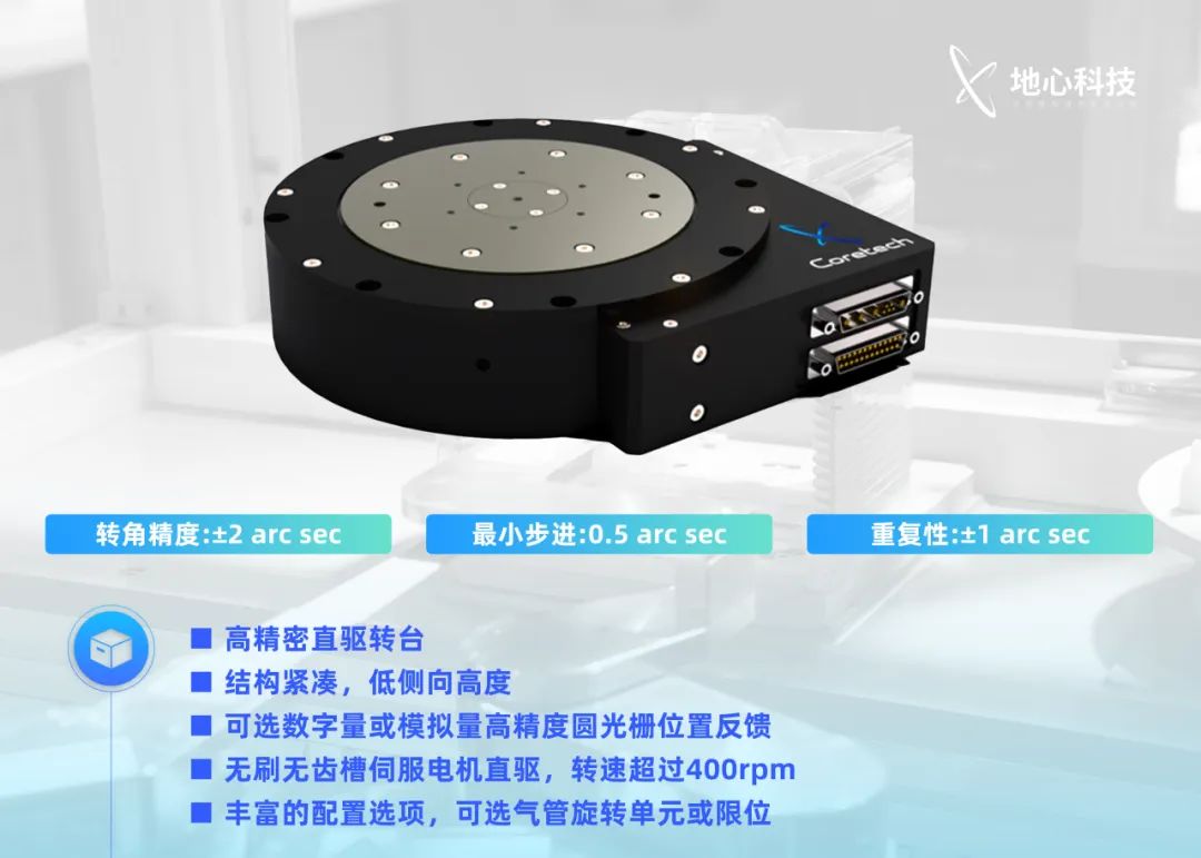
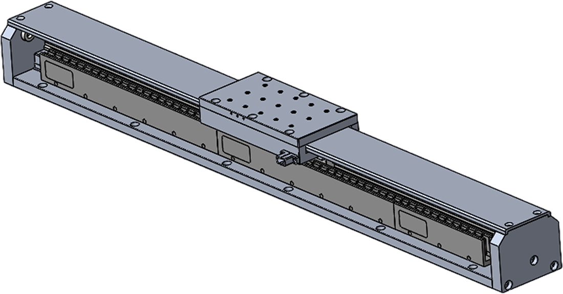
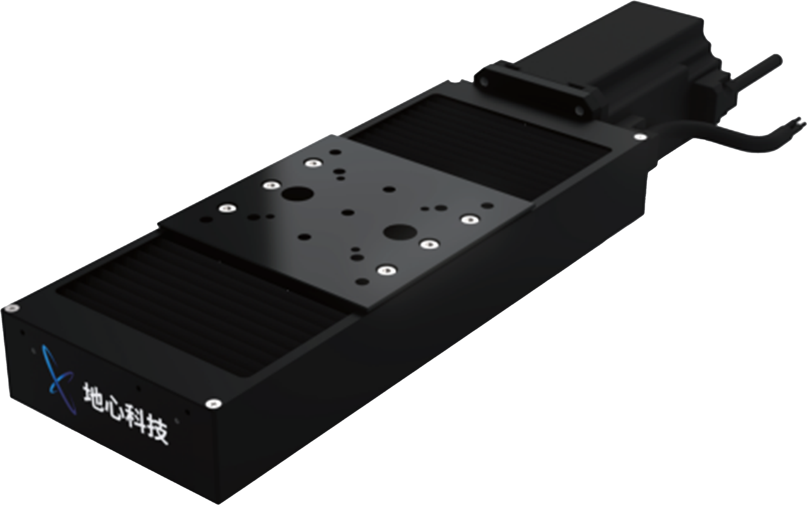
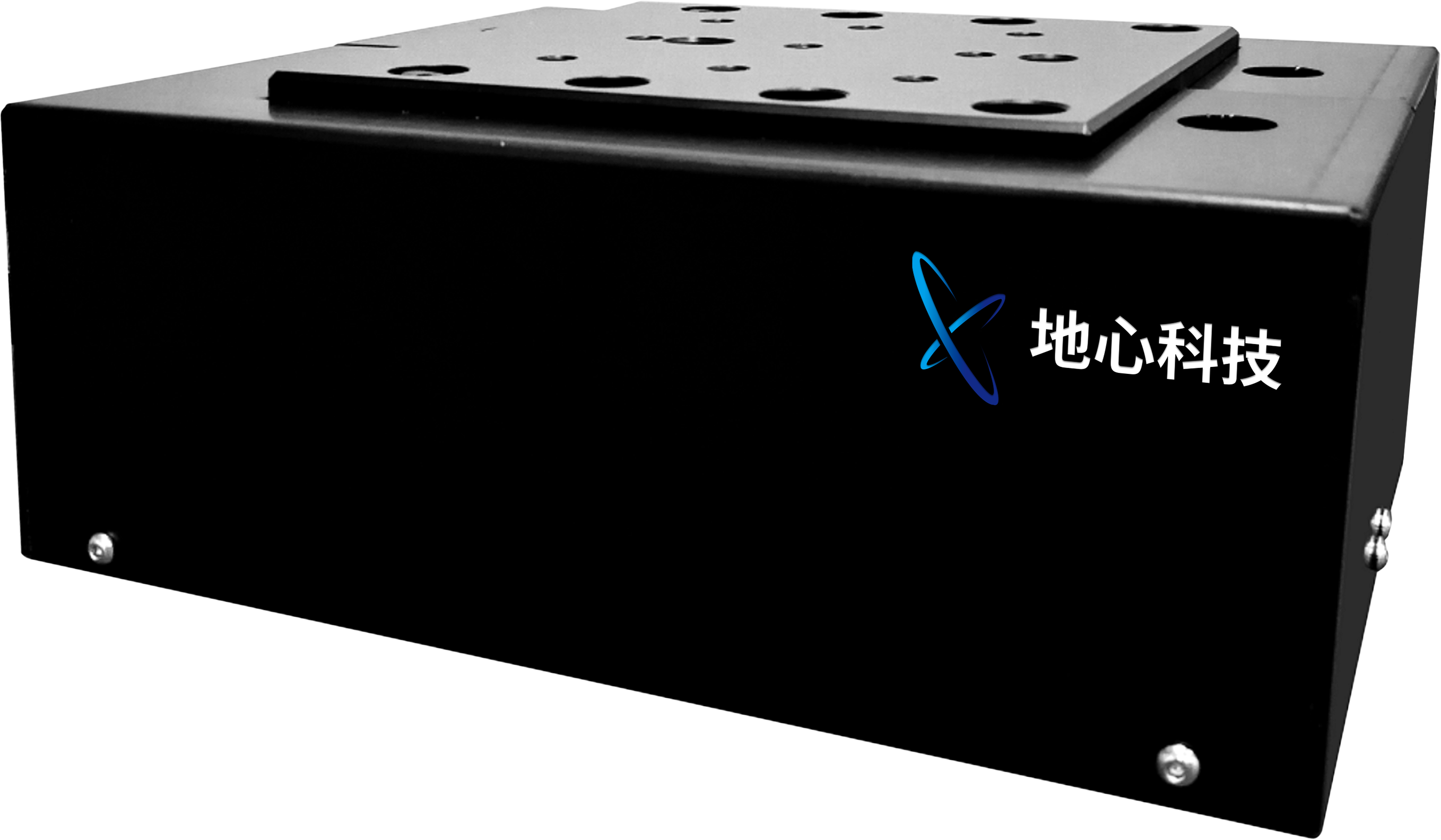
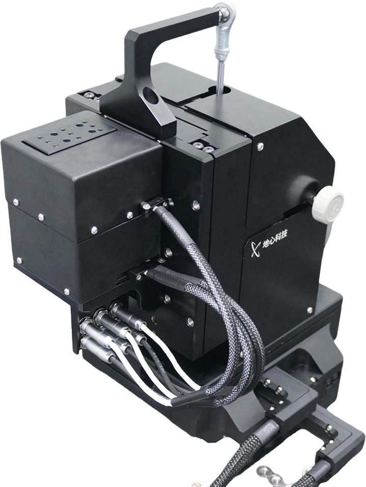
ART180 Series Linear Stages
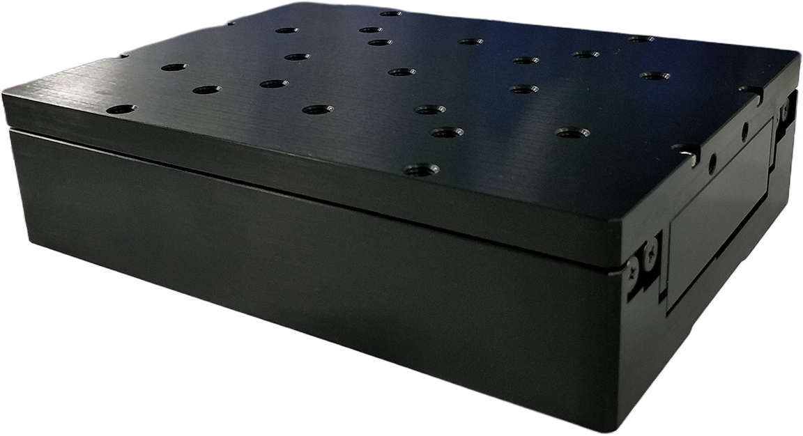
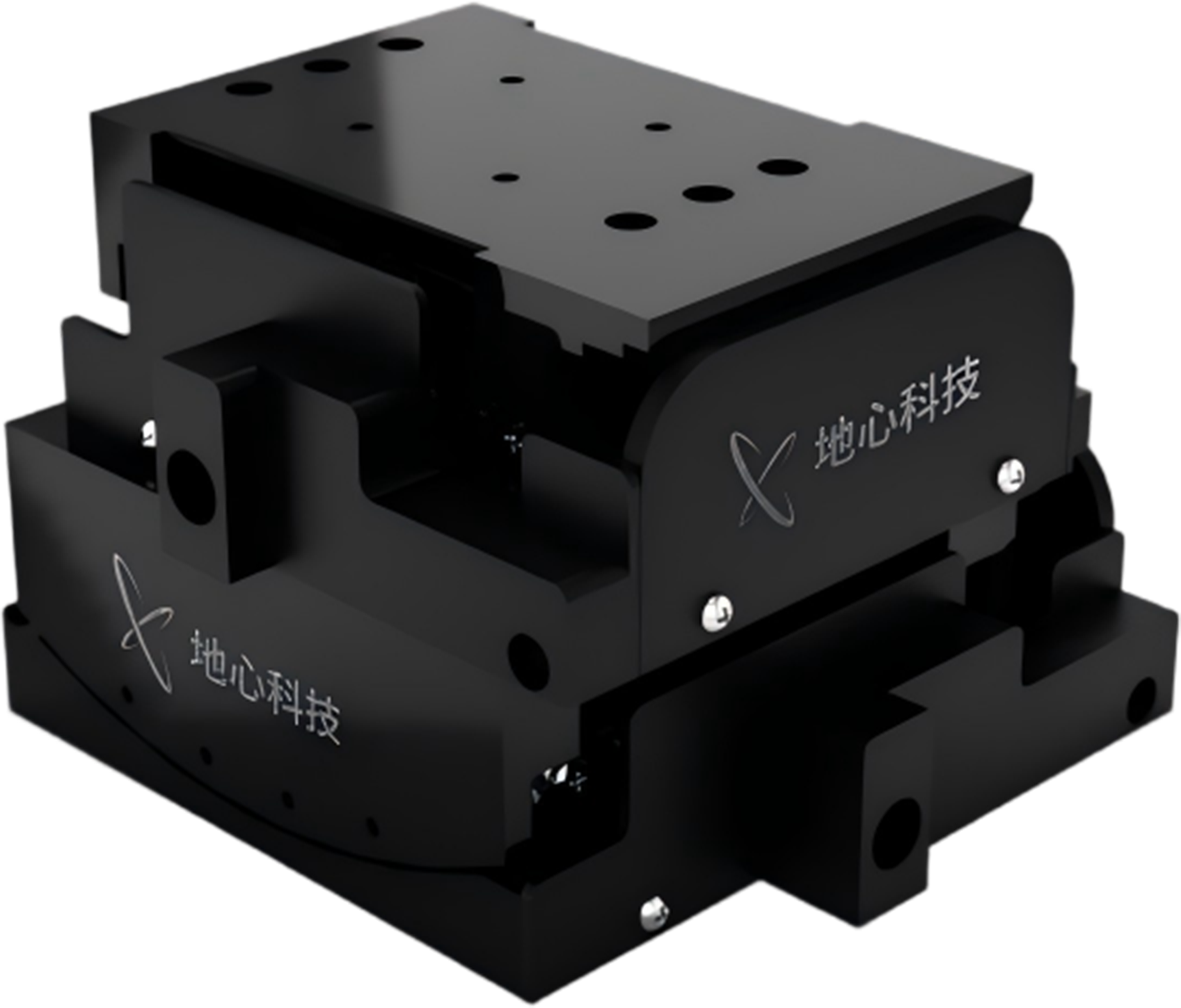
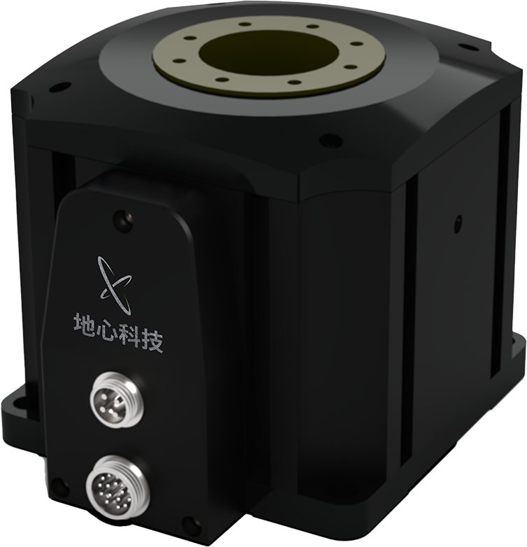
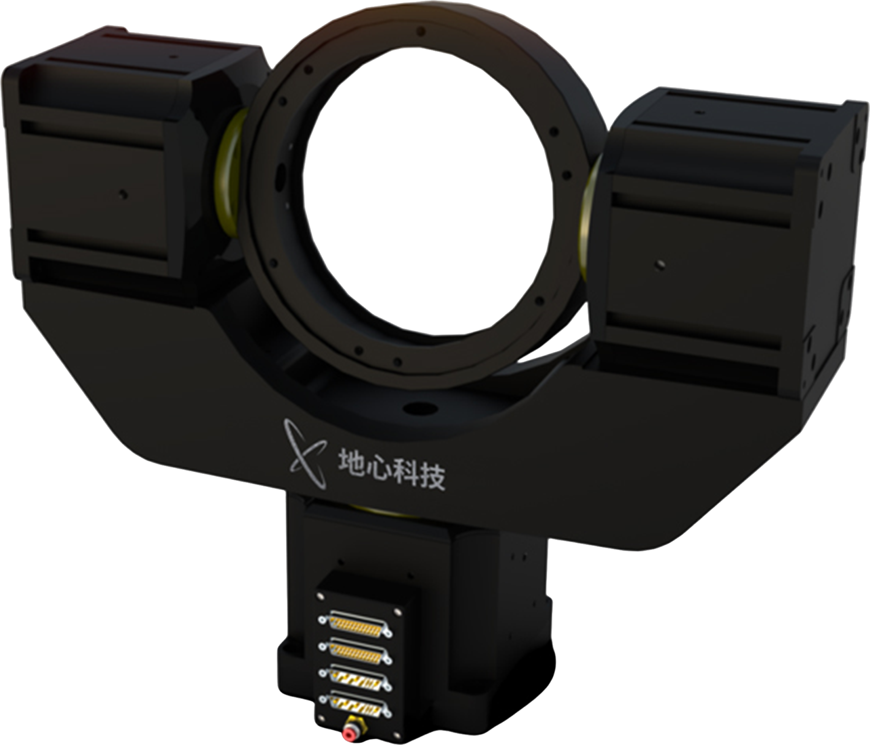
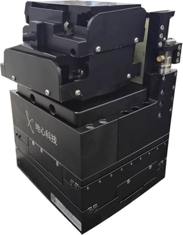
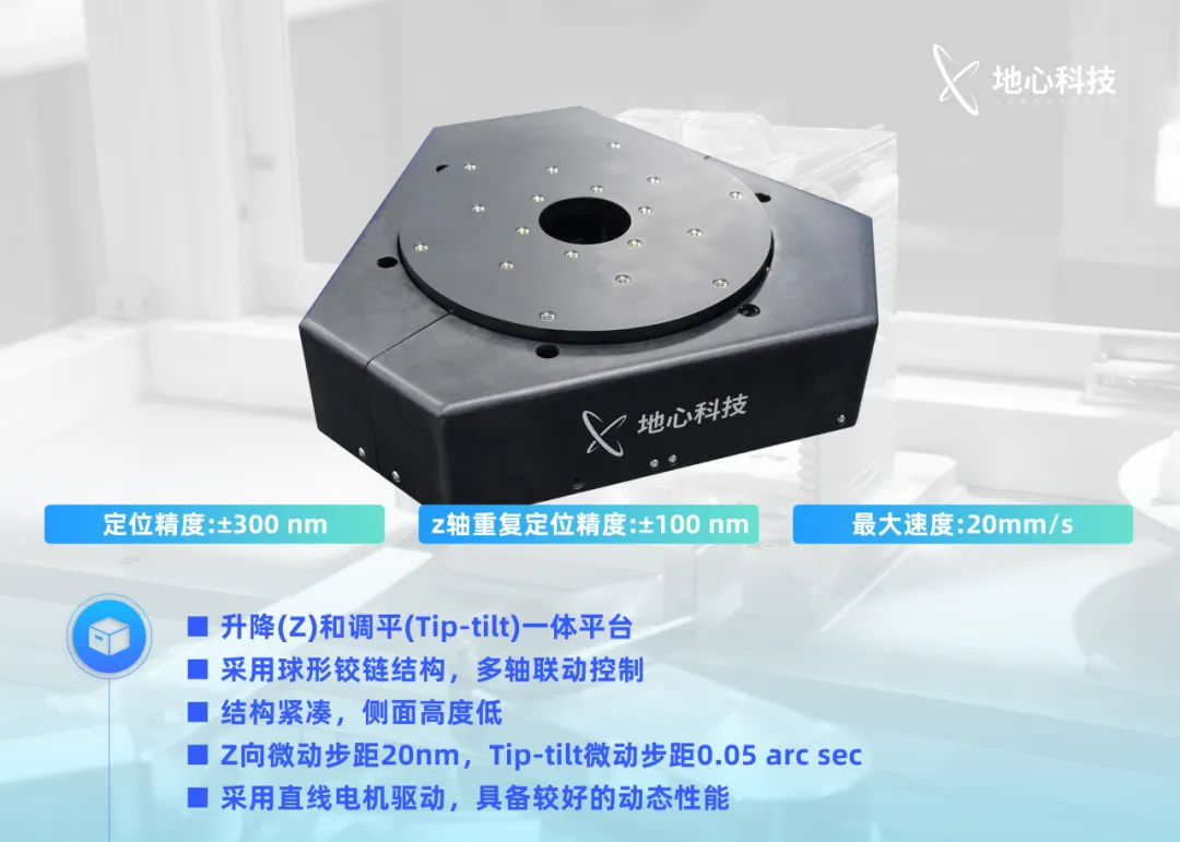
ZTT‑V2 Series Tip‑Tilt‑Z Stages
From well‑established raster scanning to high‑efficiency spiral trajectory inspection, Geocentric Technology remains committed to providing high‑performance, high‑reliability motion control solutions for both front‑end and back‑end semiconductor inspection processes. We not only offer standard products but also provide in‑depth custom development and full technical support tailored to customers' specific process and takt‑time requirements, helping the Chinese semiconductor industry achieve more precise, more efficient, and more intelligent defect inspection.
Featured News
One Article Summary | Multiple Applications of Precision Motion Stages in Wafer Defect Inspection
2026.06.03
Laser Processing Automation Solutions – Laser Micro/Nano Machining
2026.06.03
Improving Yield and Efficiency: High‑Precision Motion Stages Empowering Innovation in Laser Direct Writing Technology
2026.06.03
 Back to List