
.png)

.png)

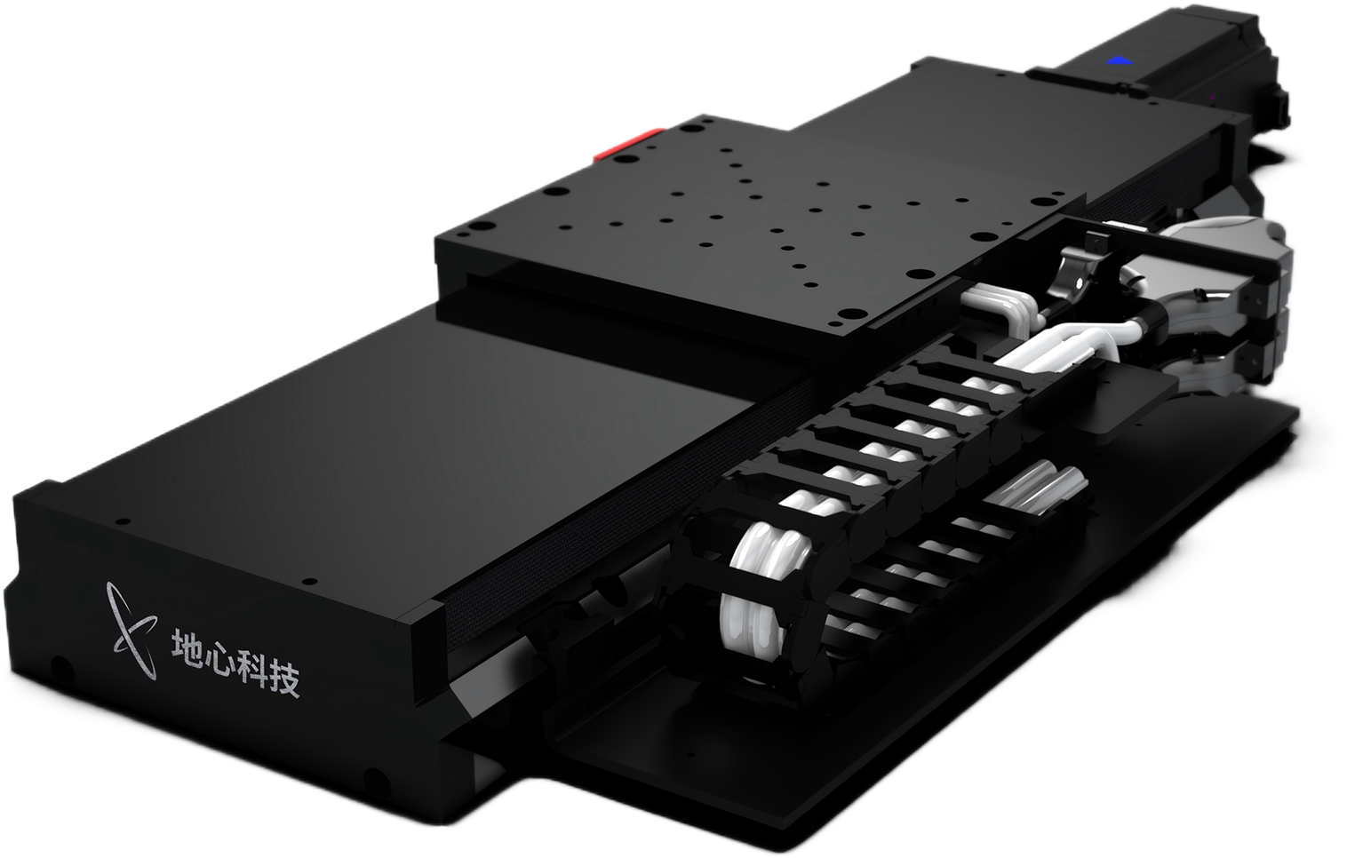
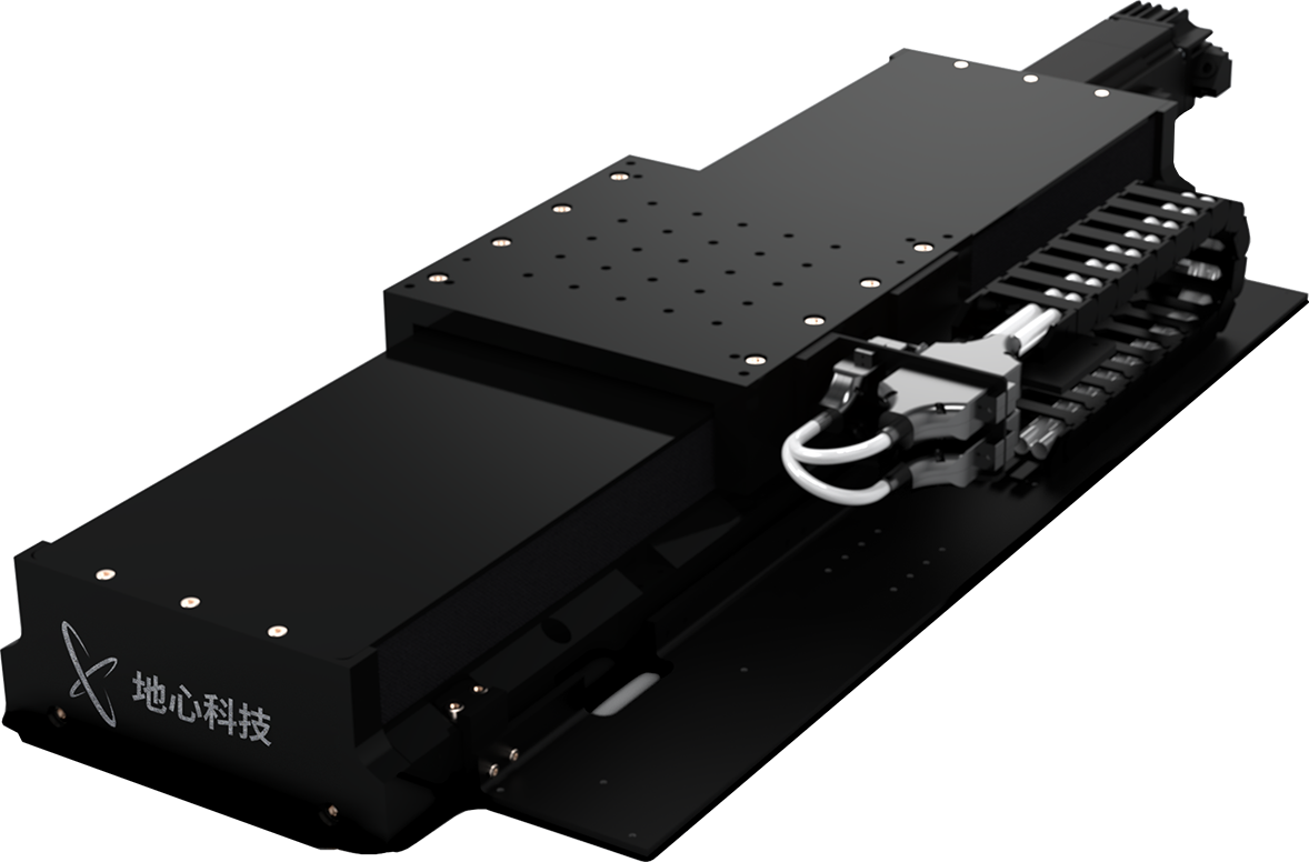
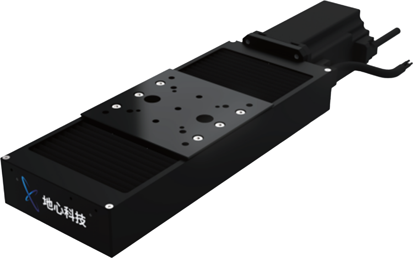
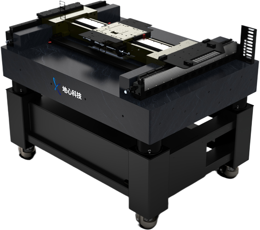
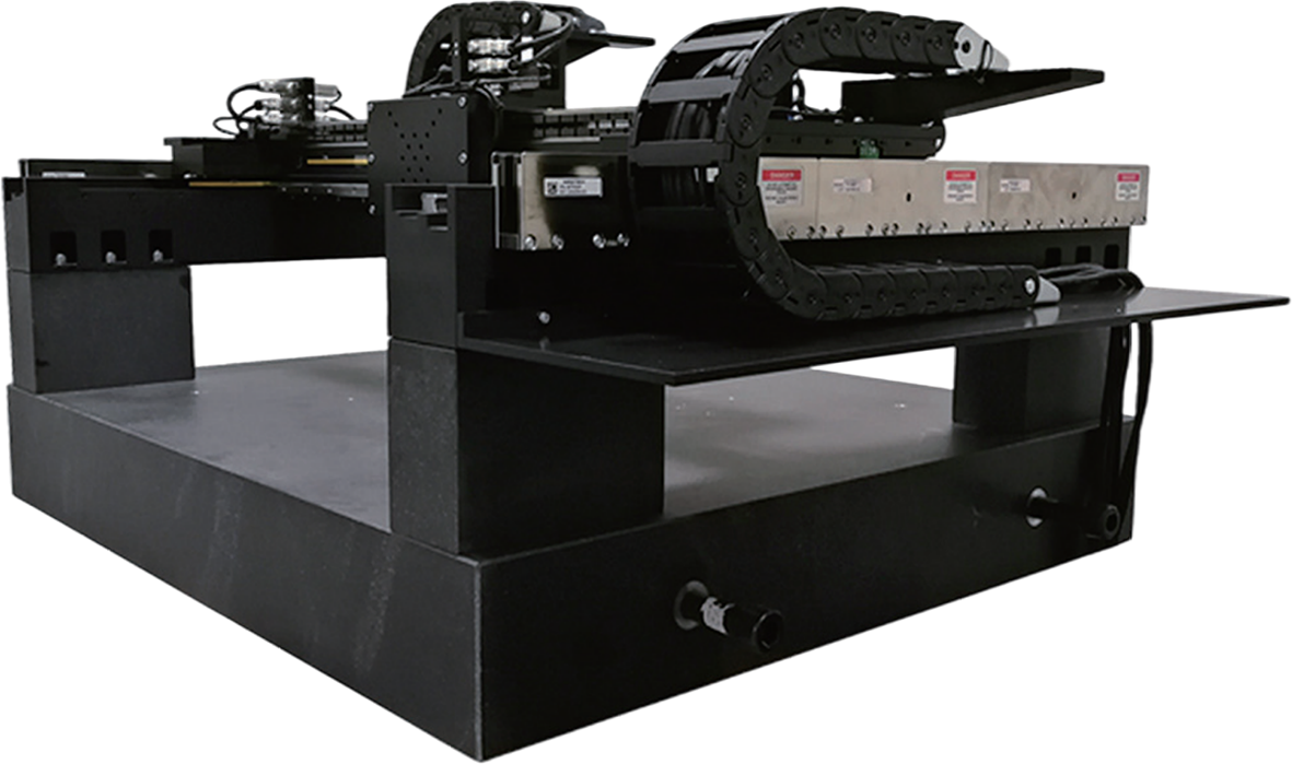
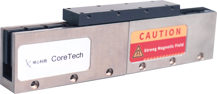
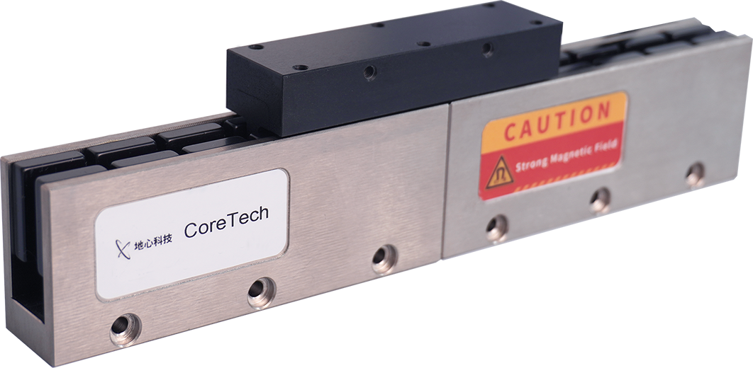
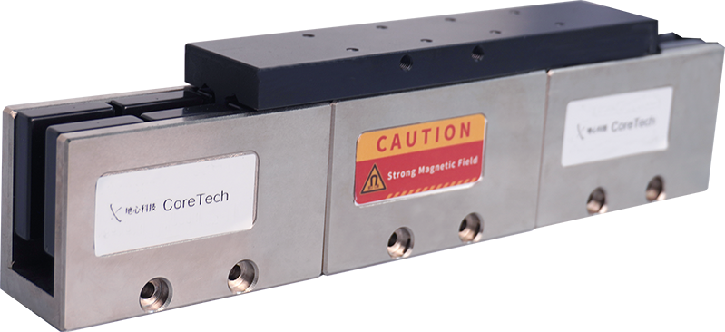
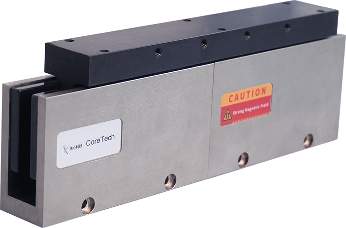
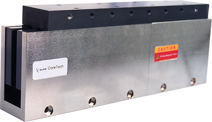
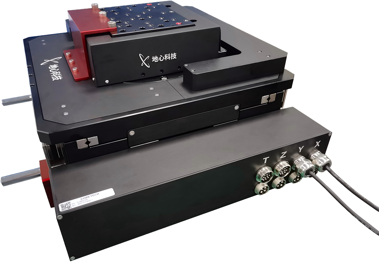




Wafer Defect Inspection
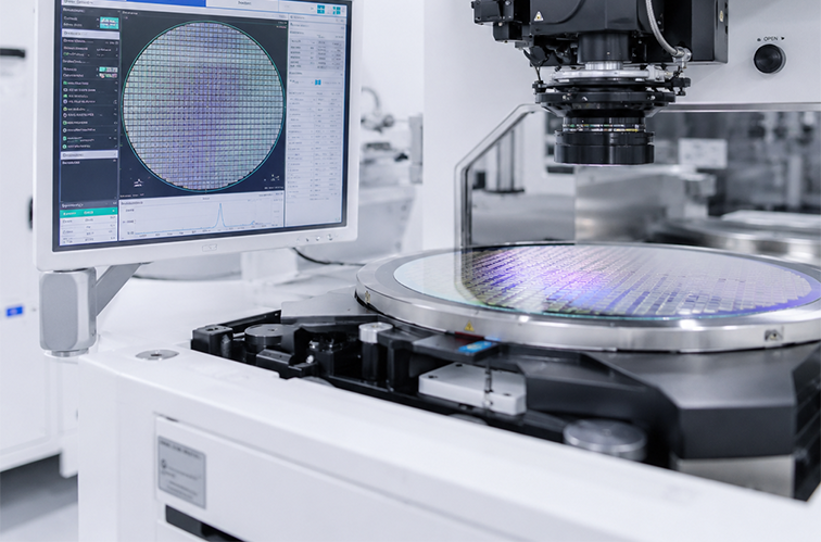
Semiconductor manufacturing involves complex processes, and rigorous inspection is required at nearly every step to ensure quality. Defective dies that slip through to subsequent stages not only compromise overall product quality but also drive up production costs significantly.
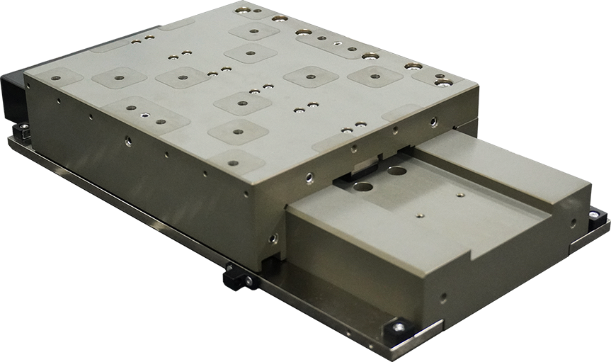
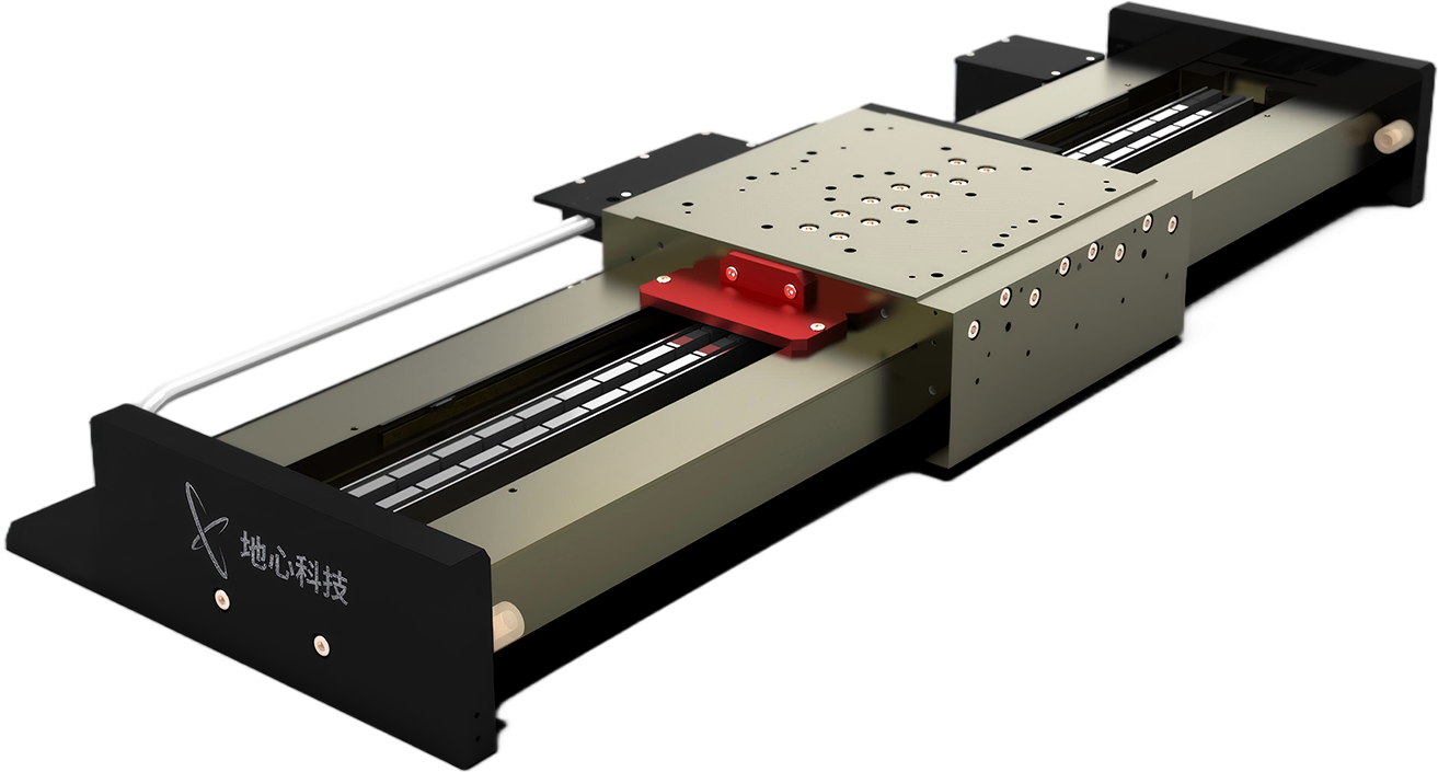
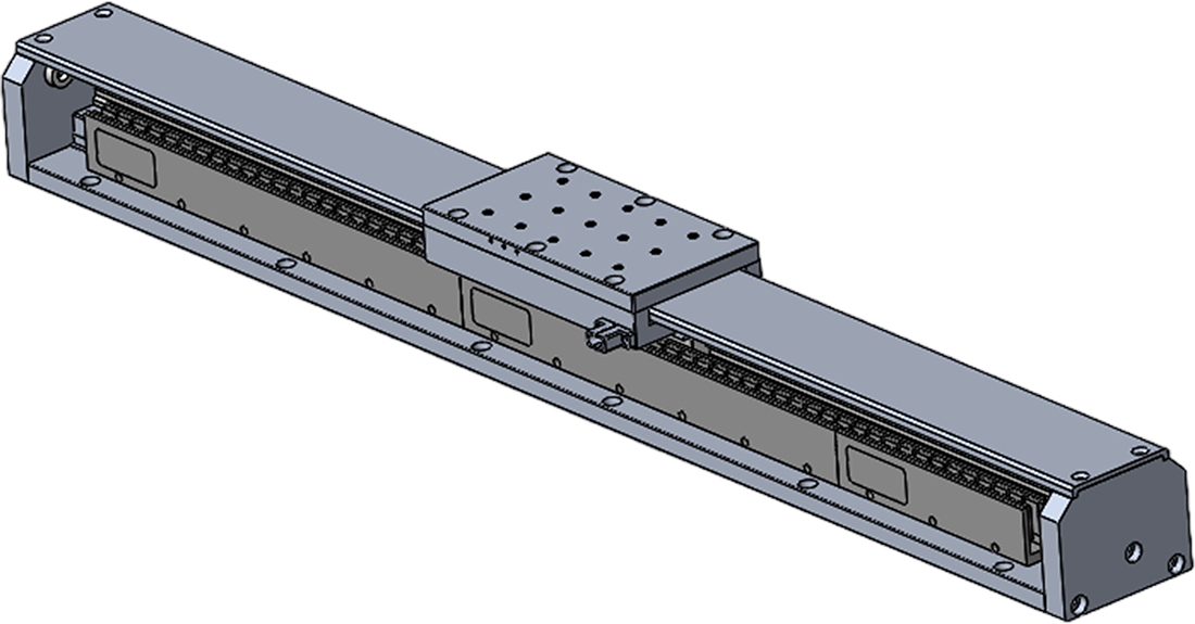
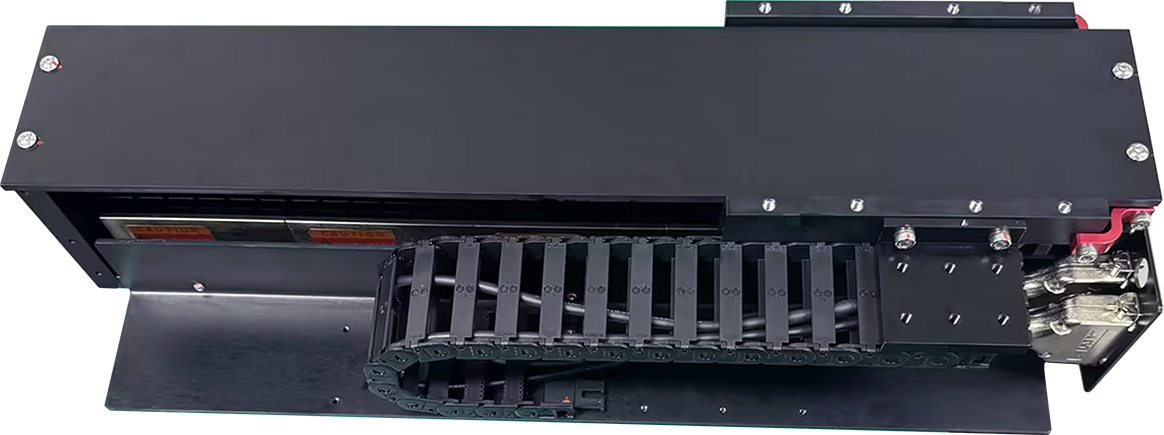
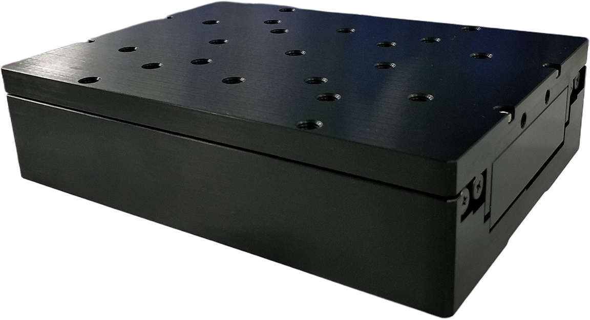
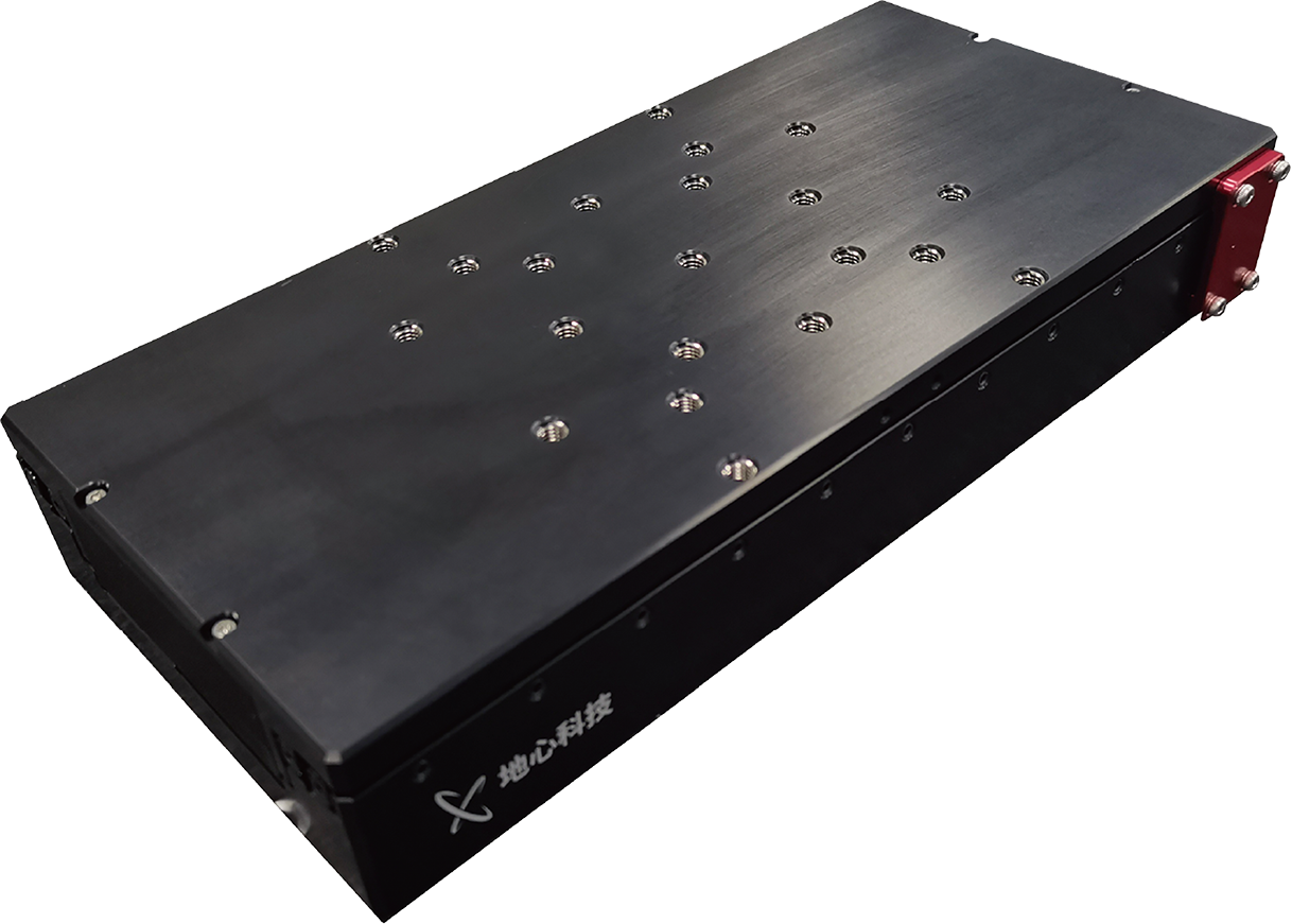
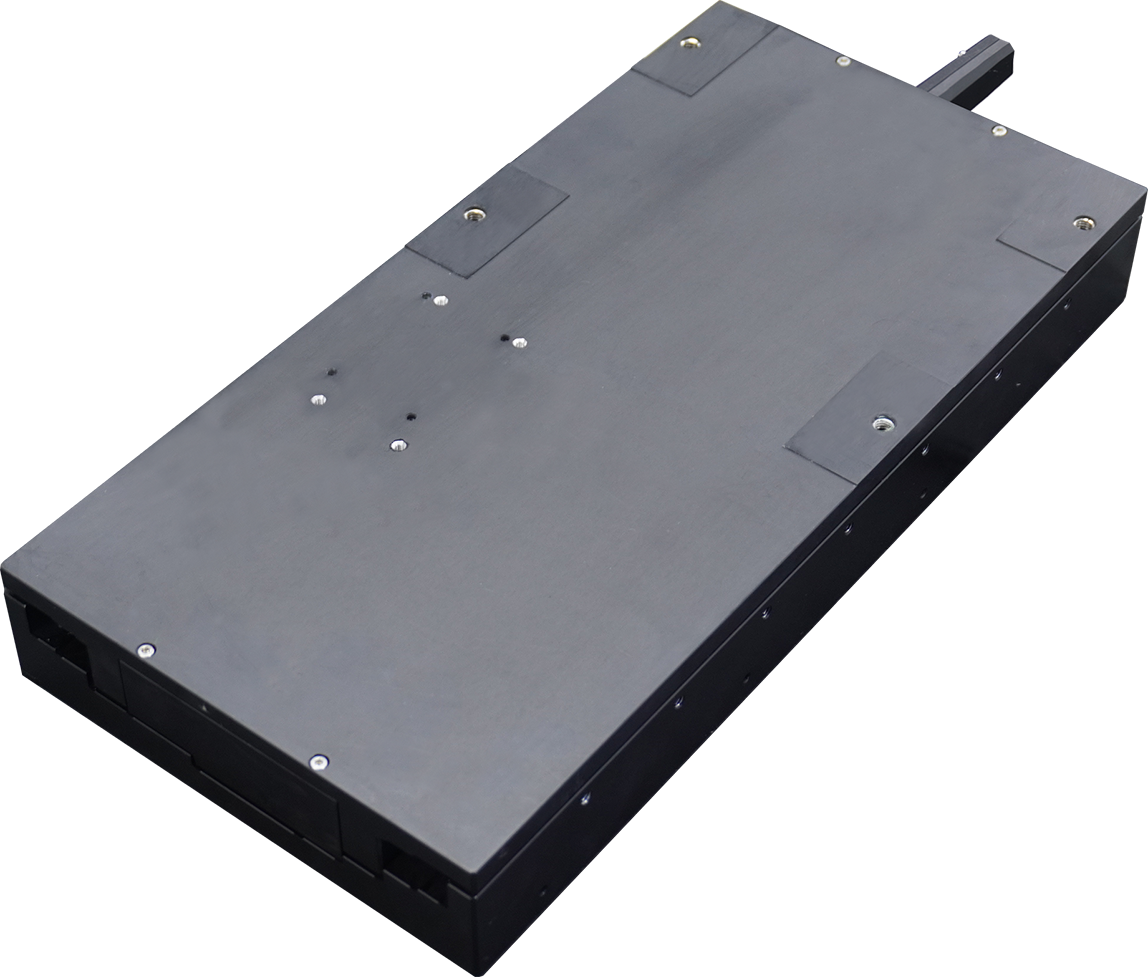
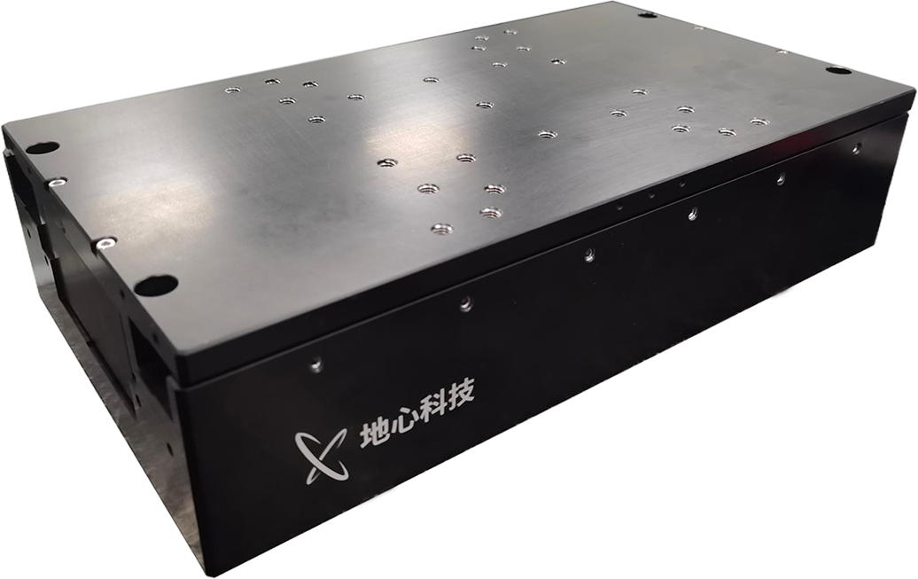
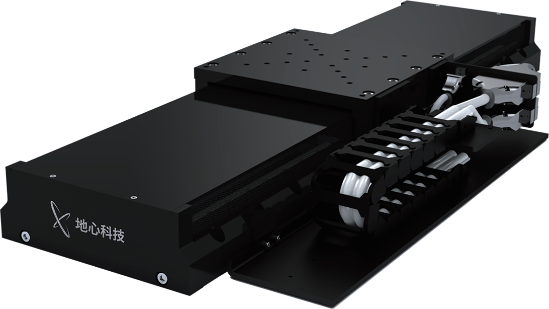
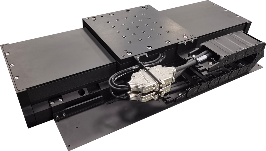
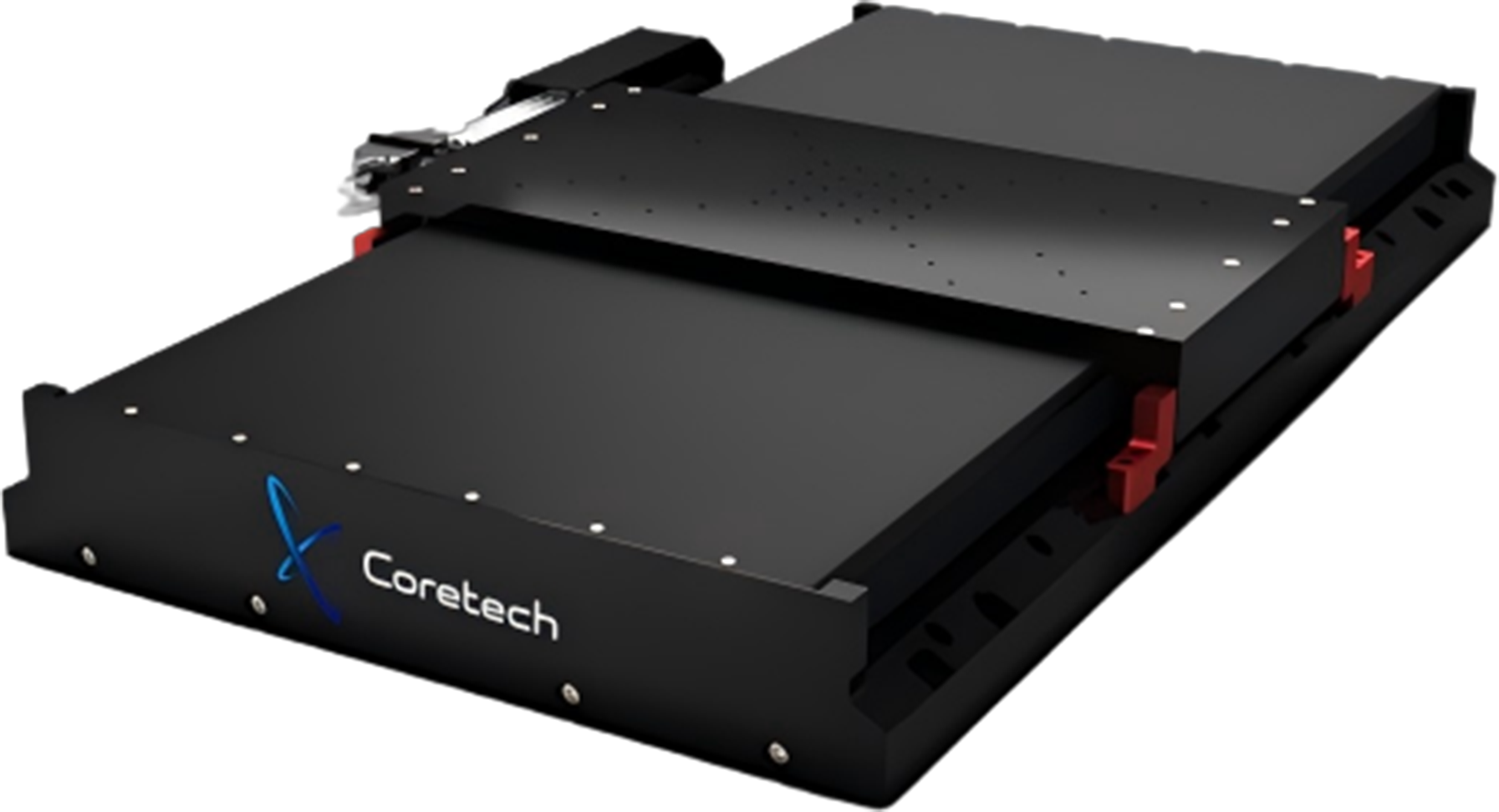
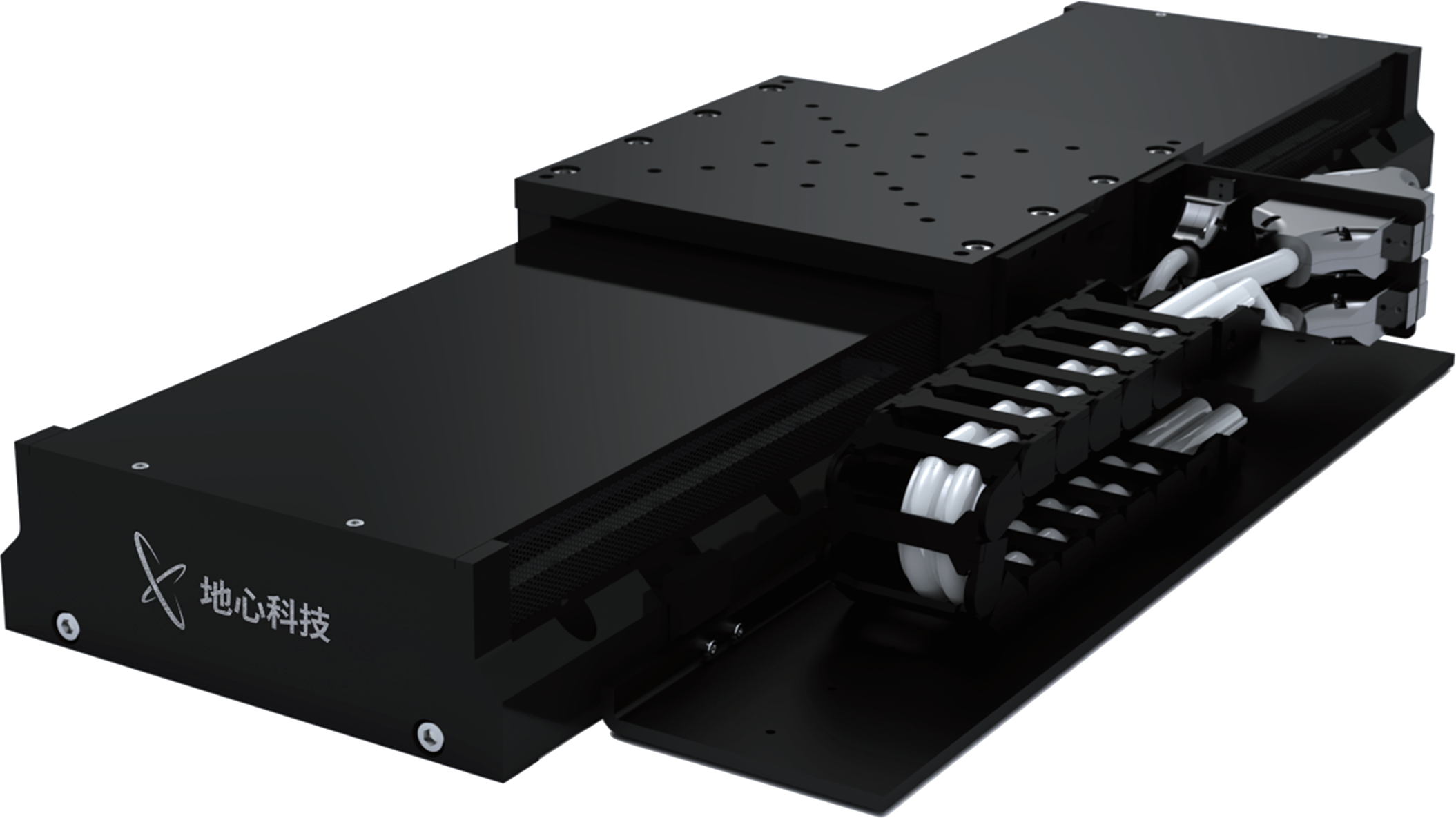
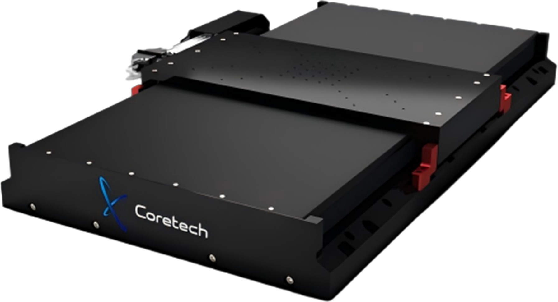
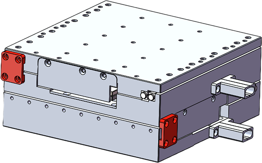
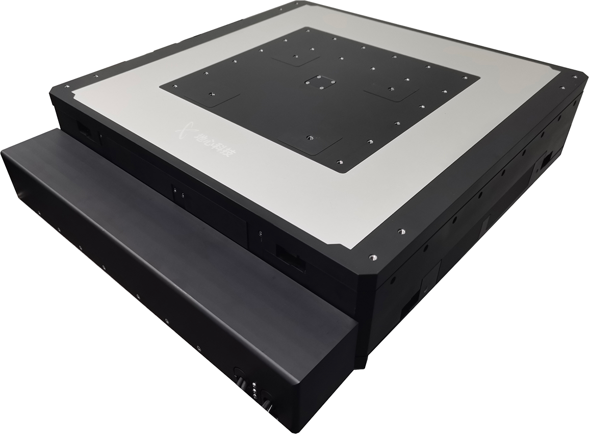
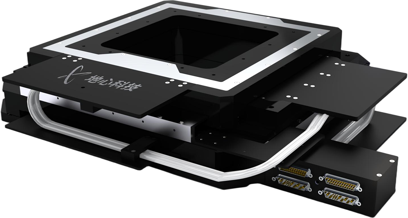
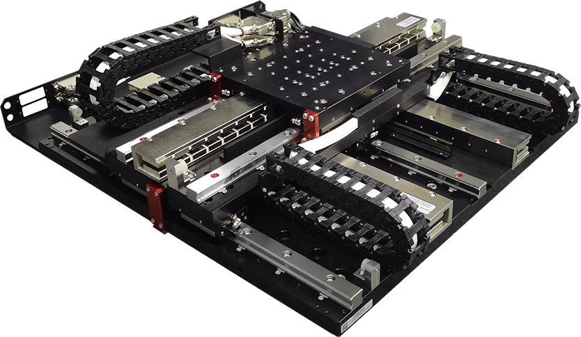
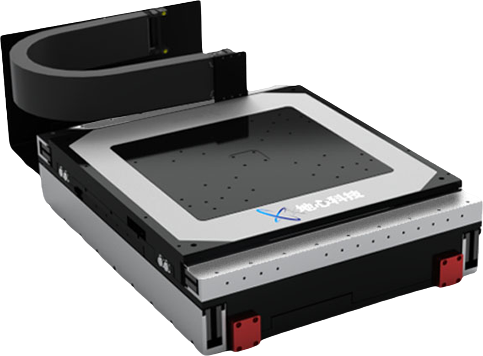
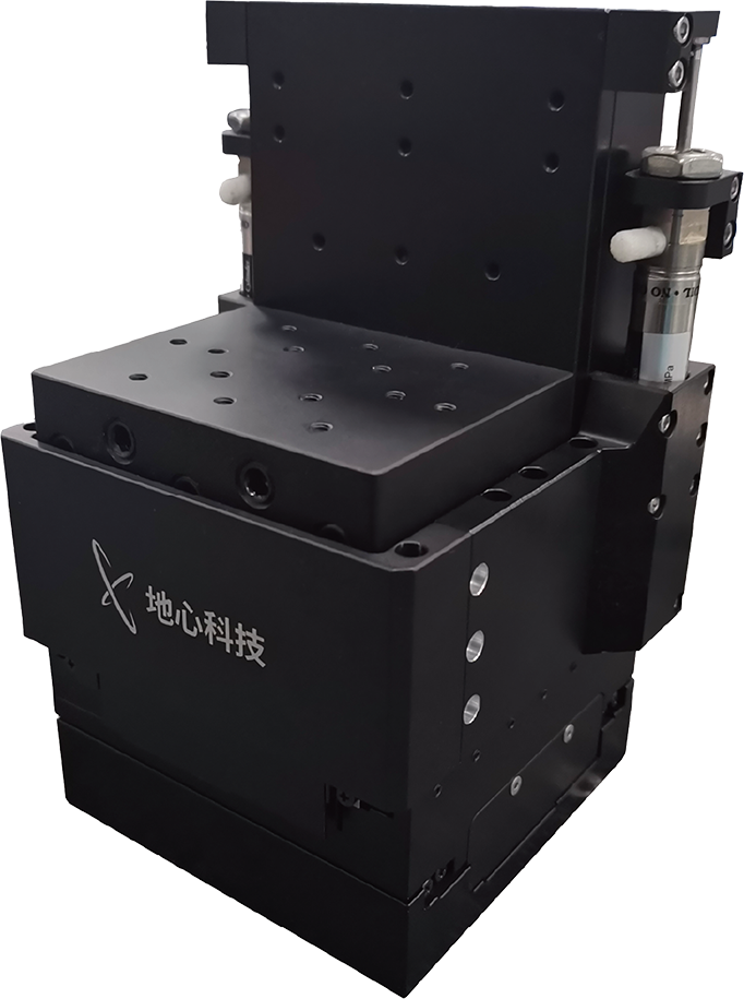
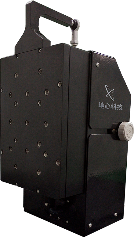
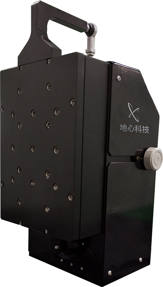
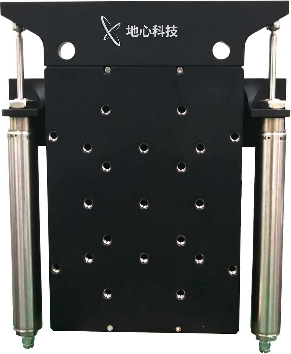
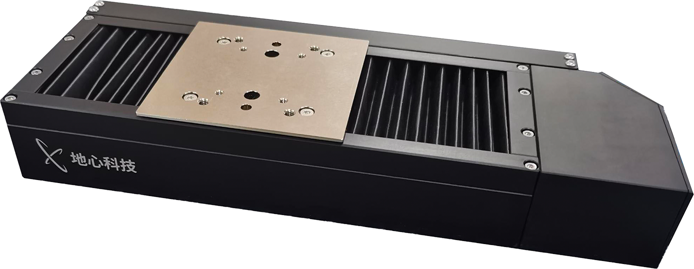
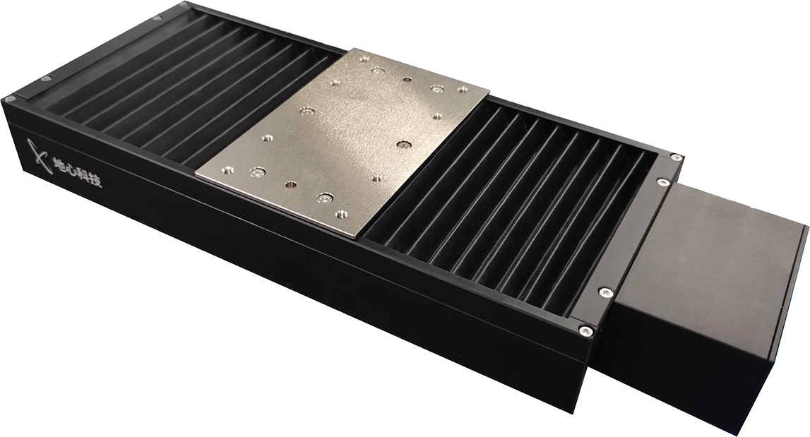
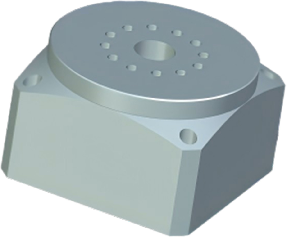
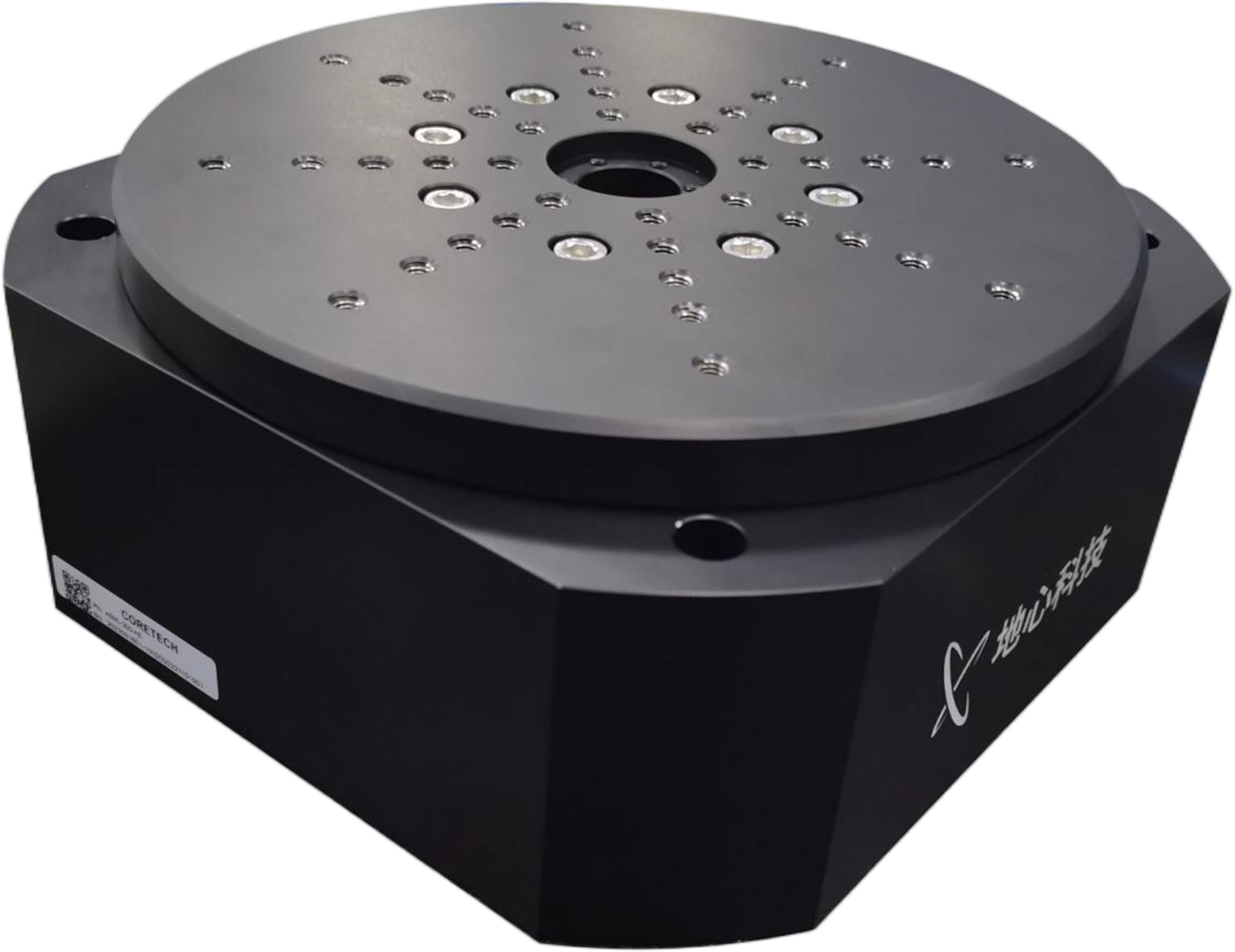
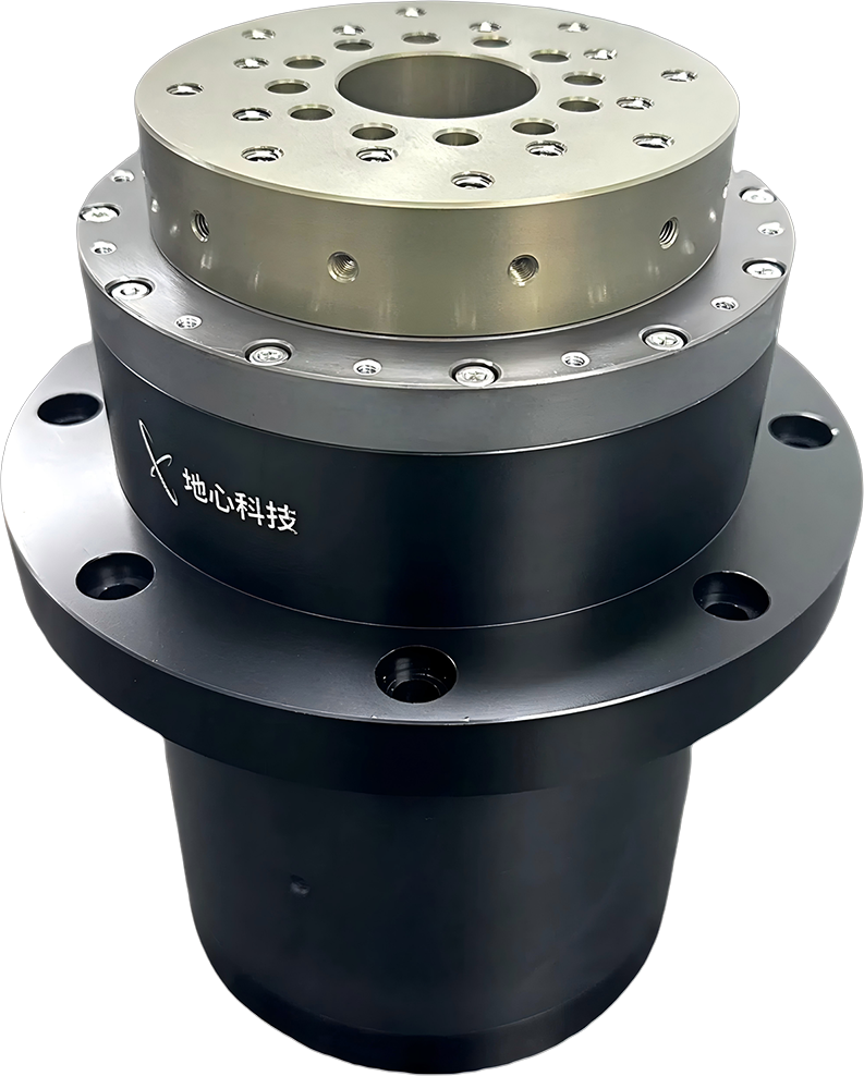
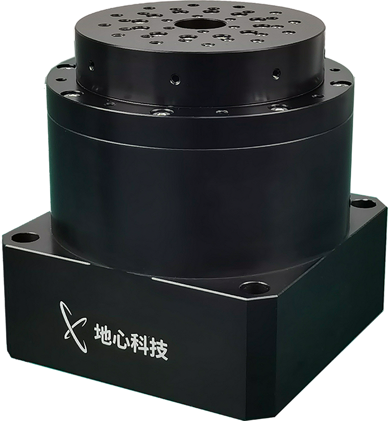
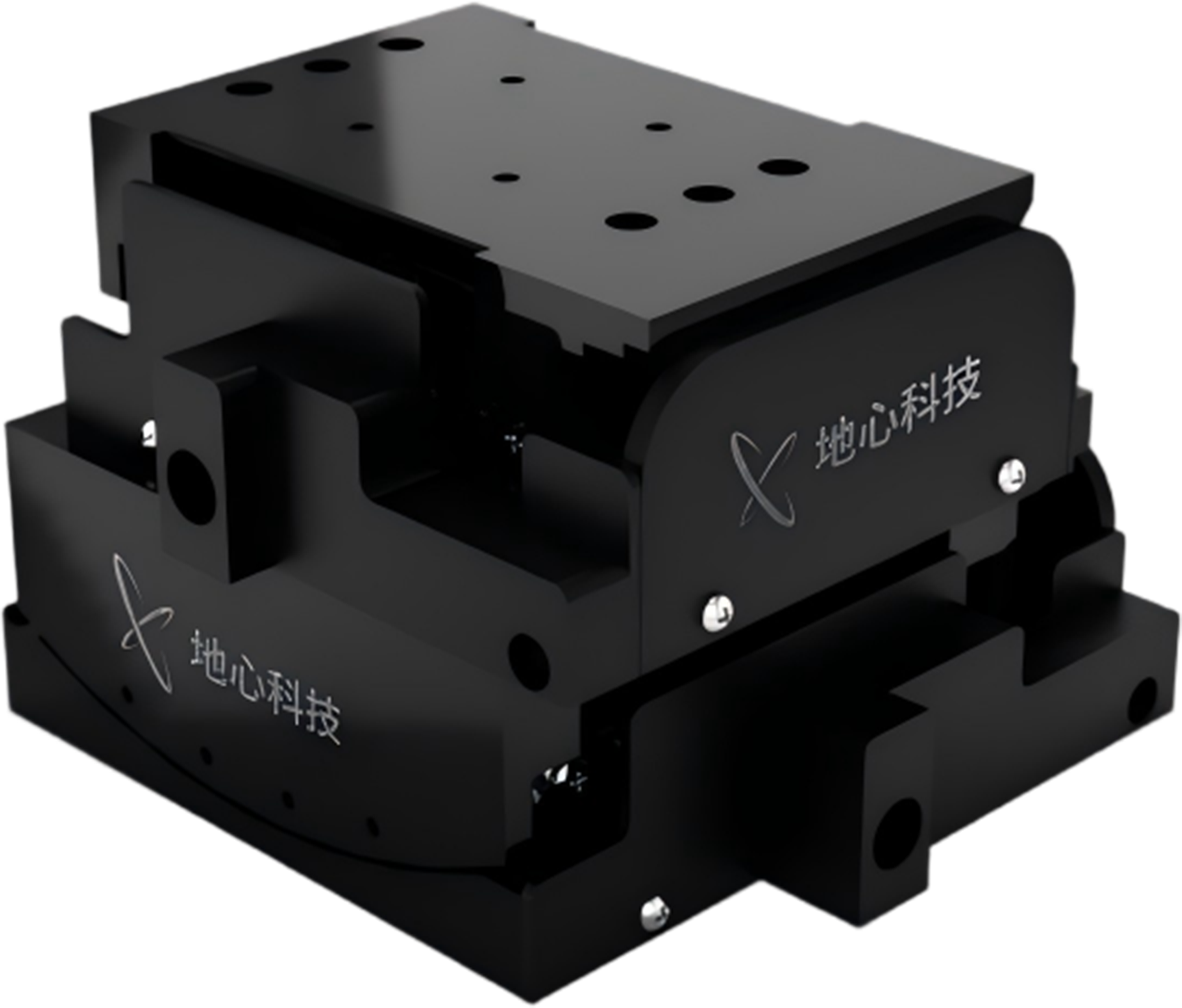
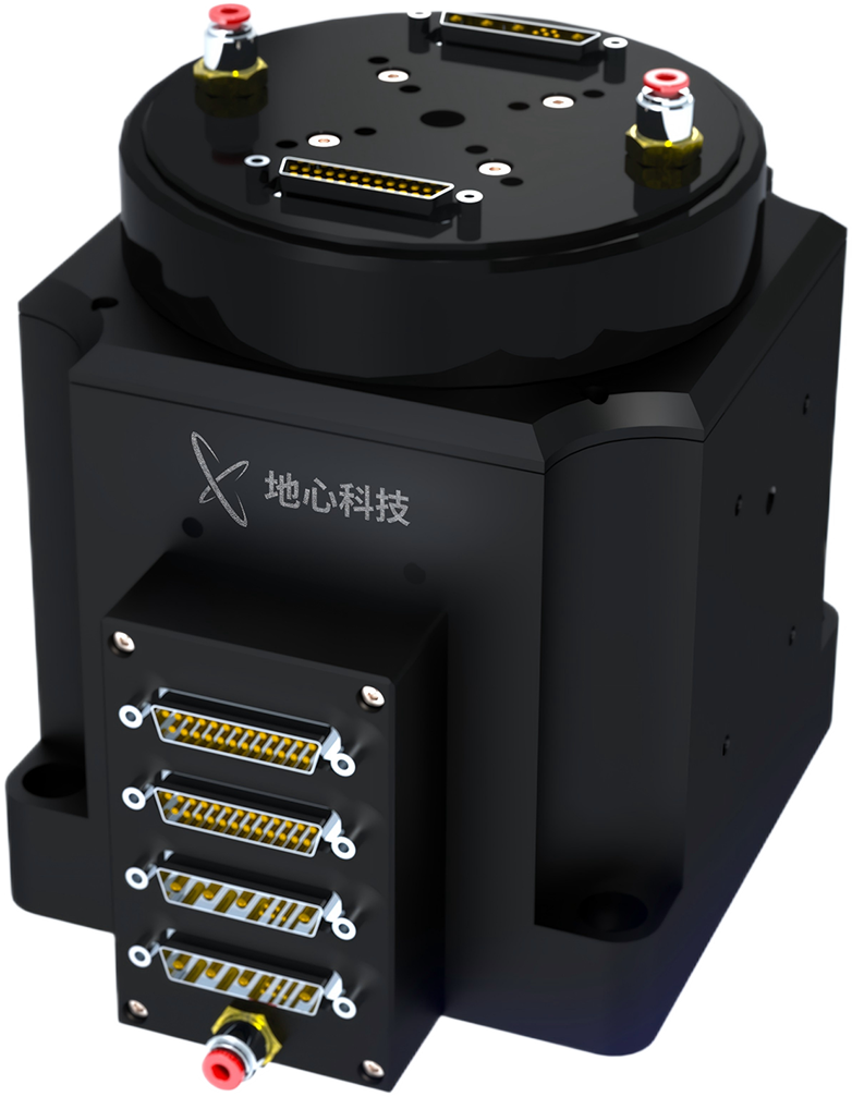
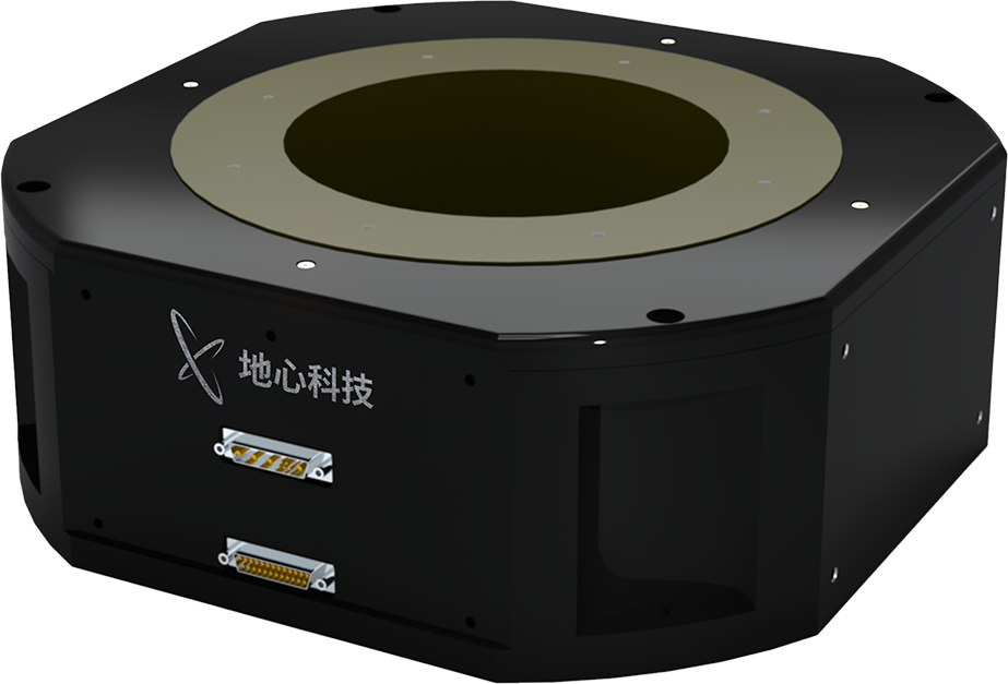
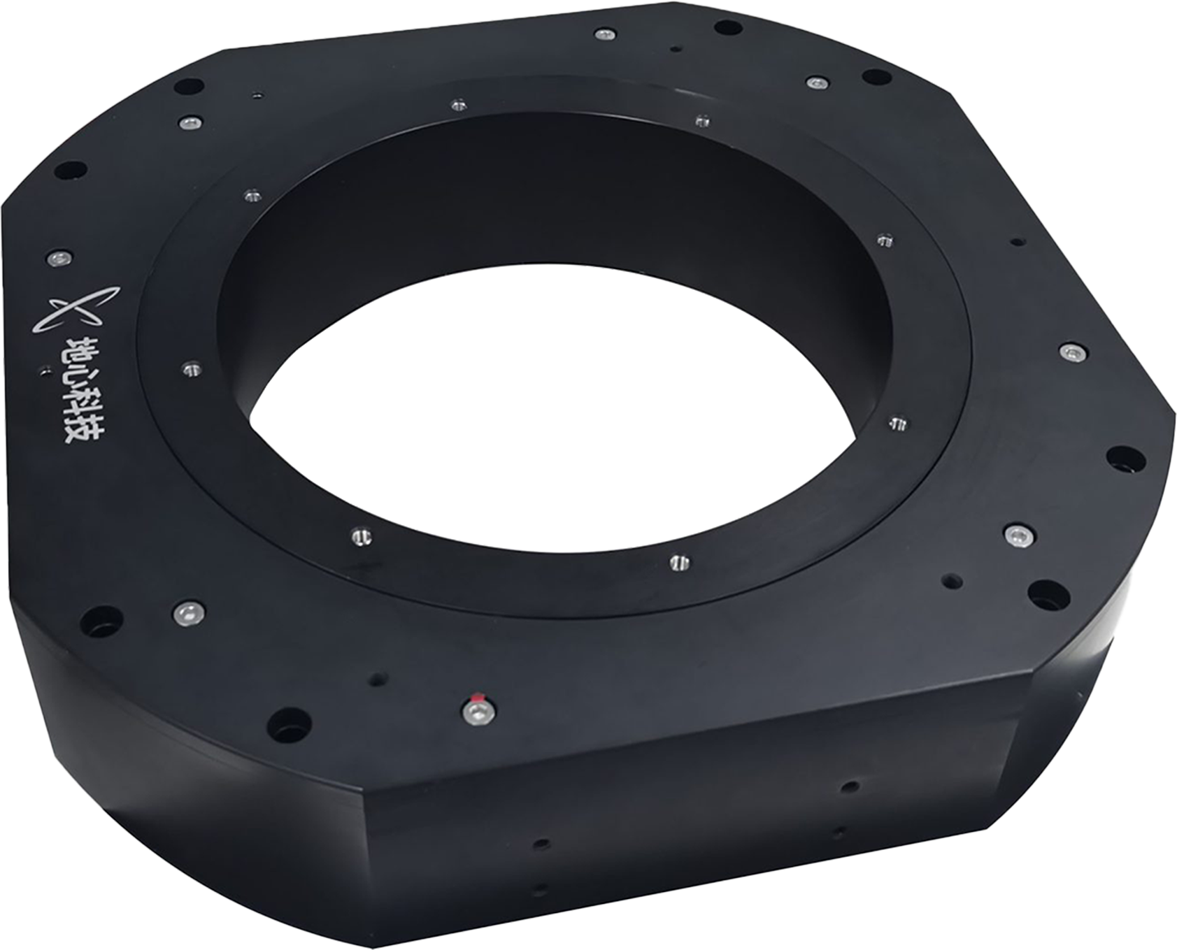
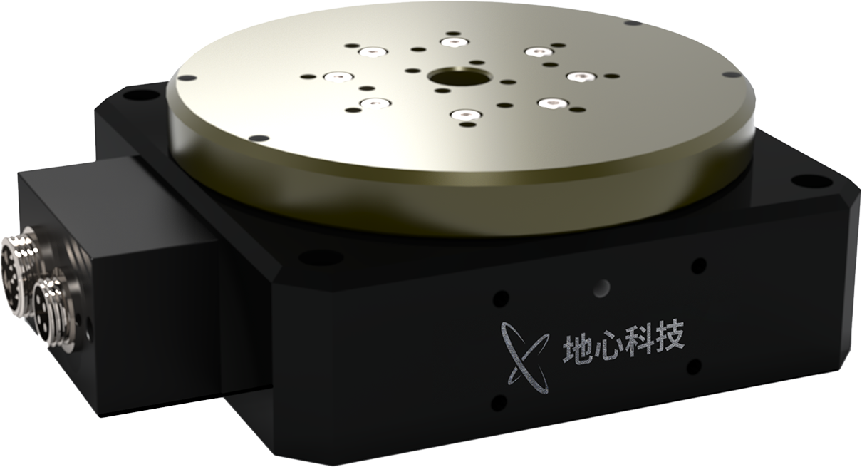
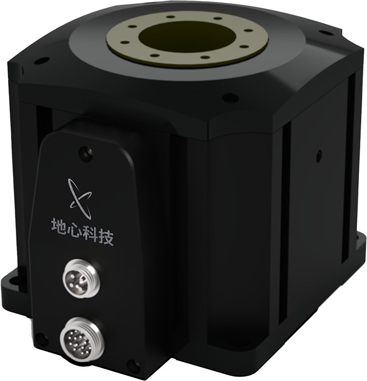
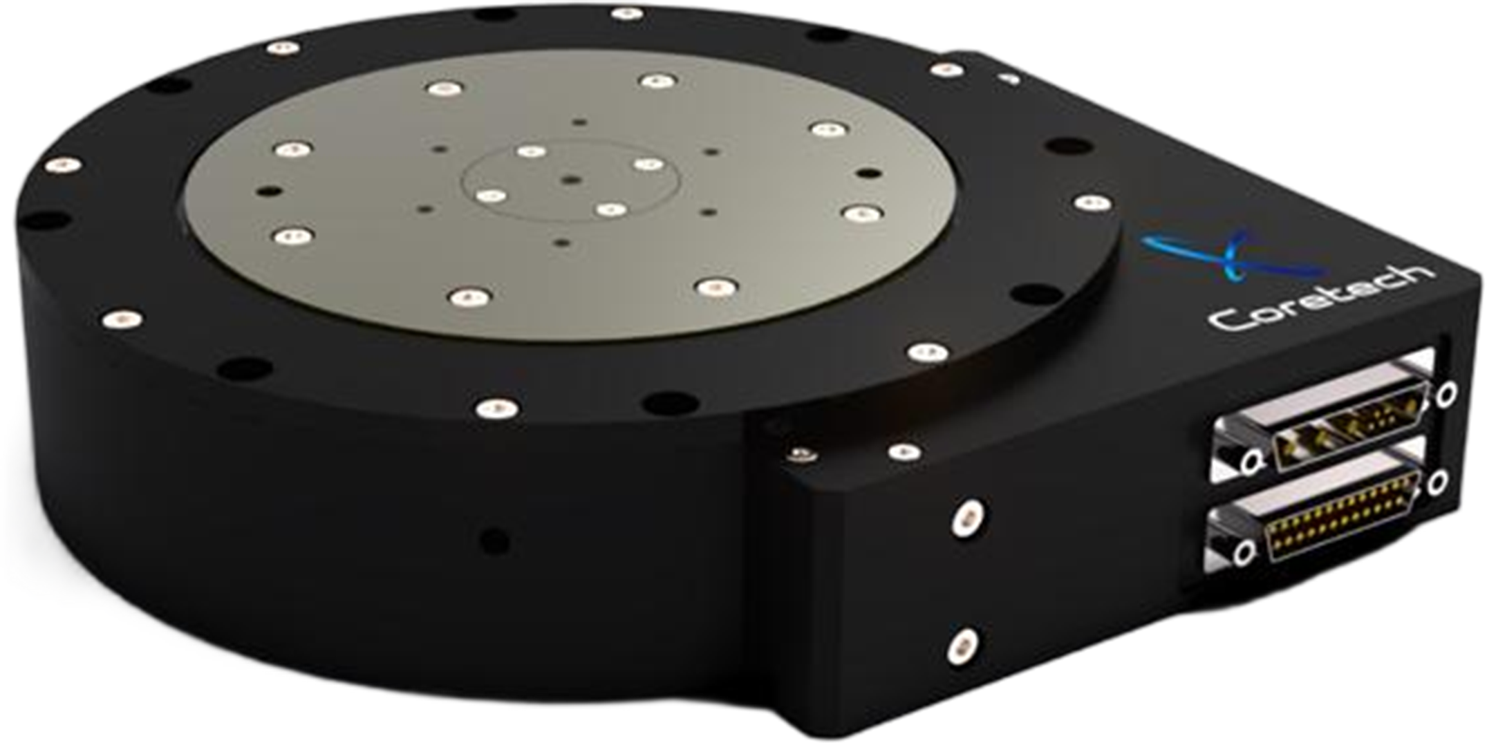
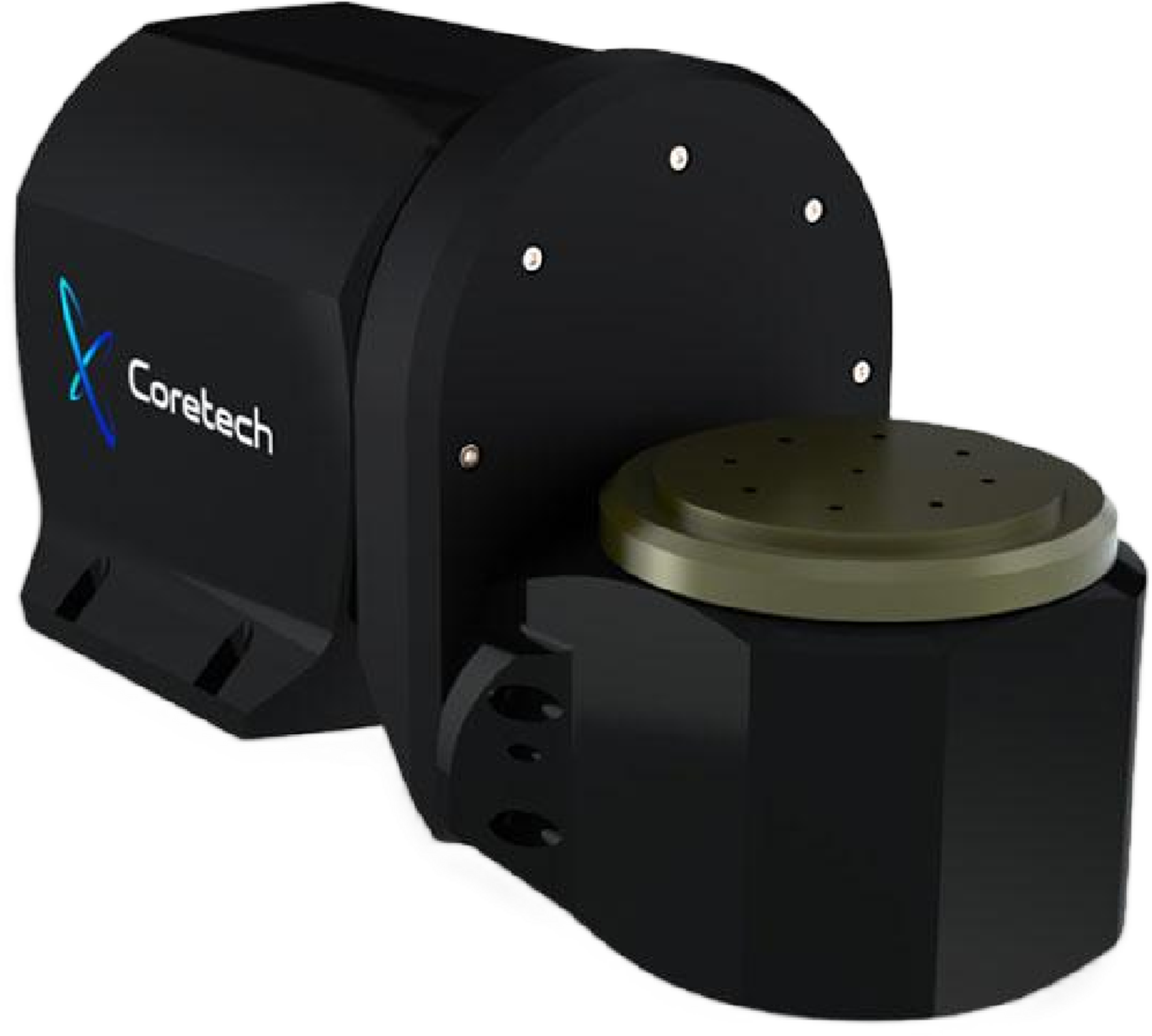
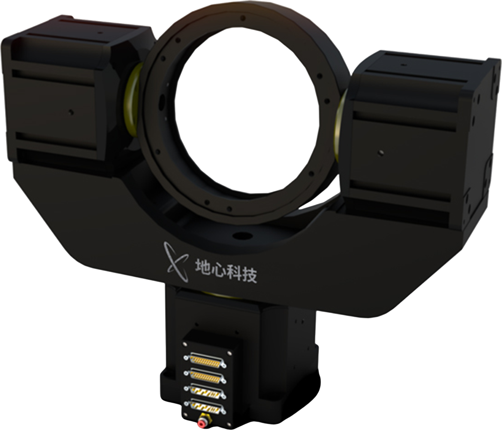
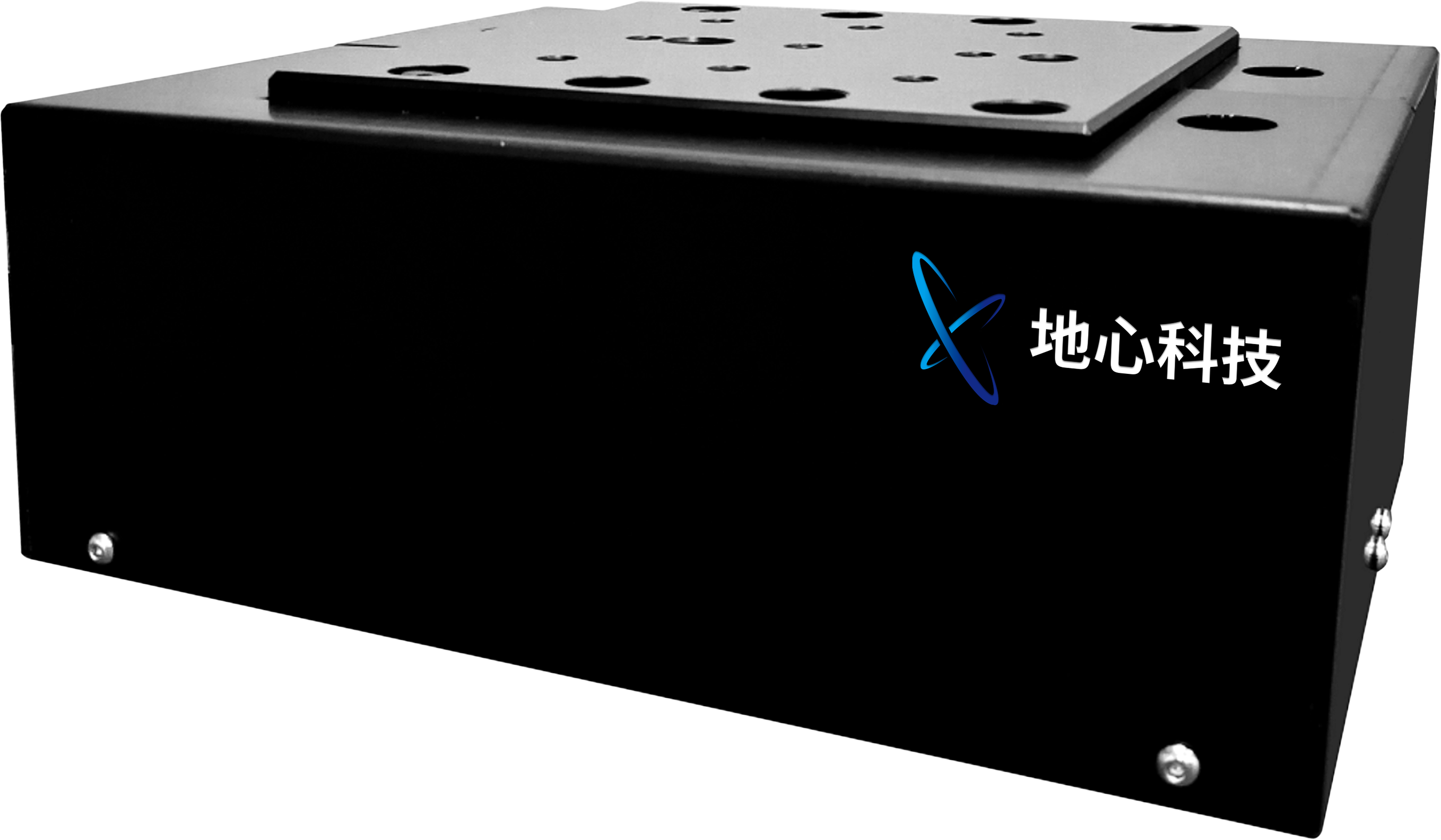
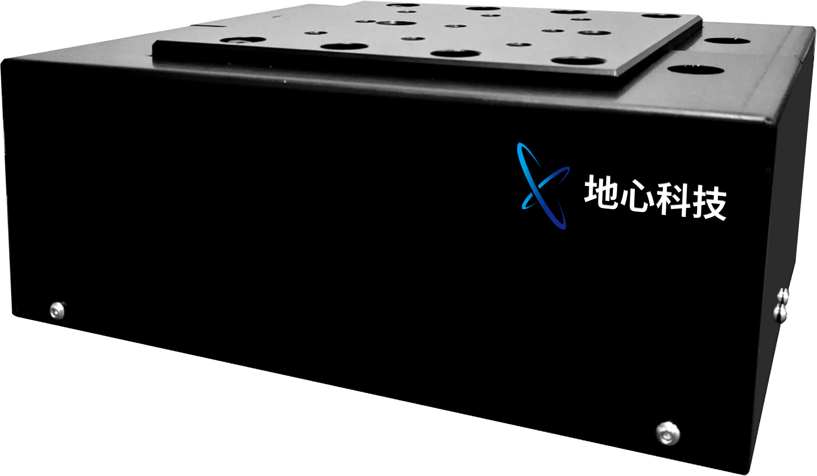
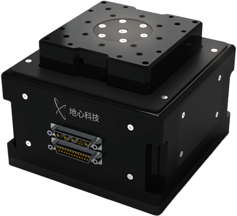
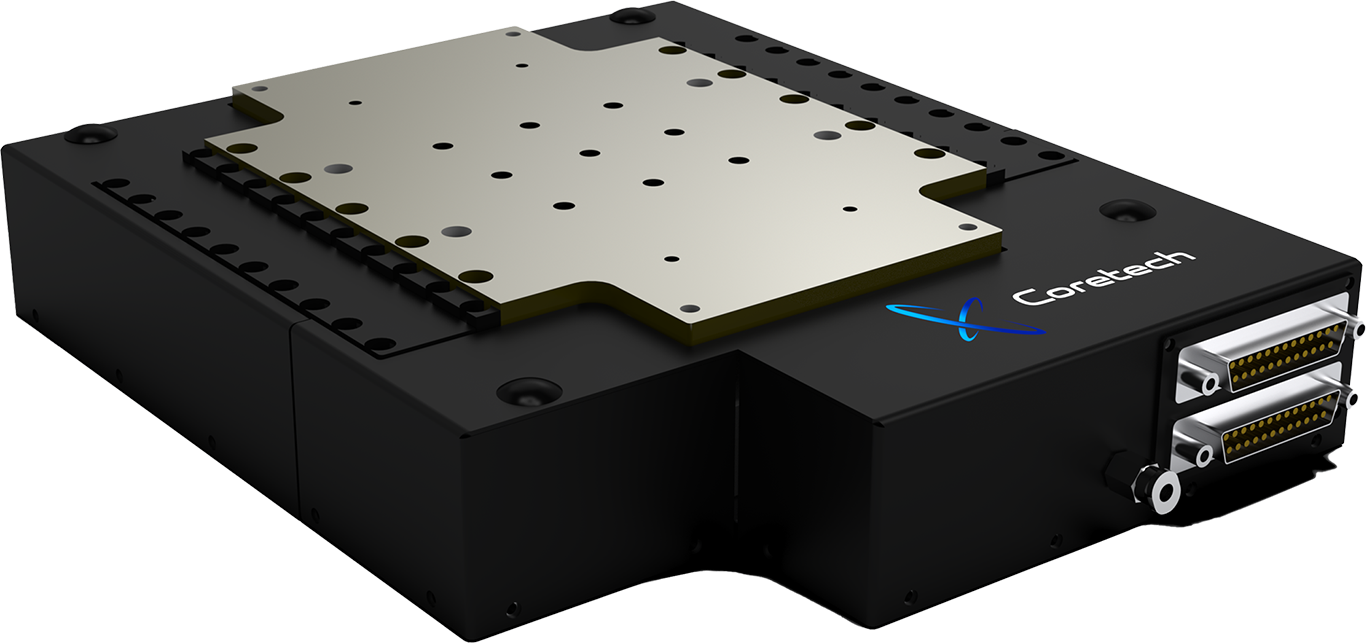
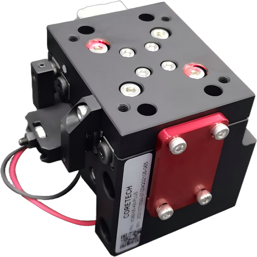
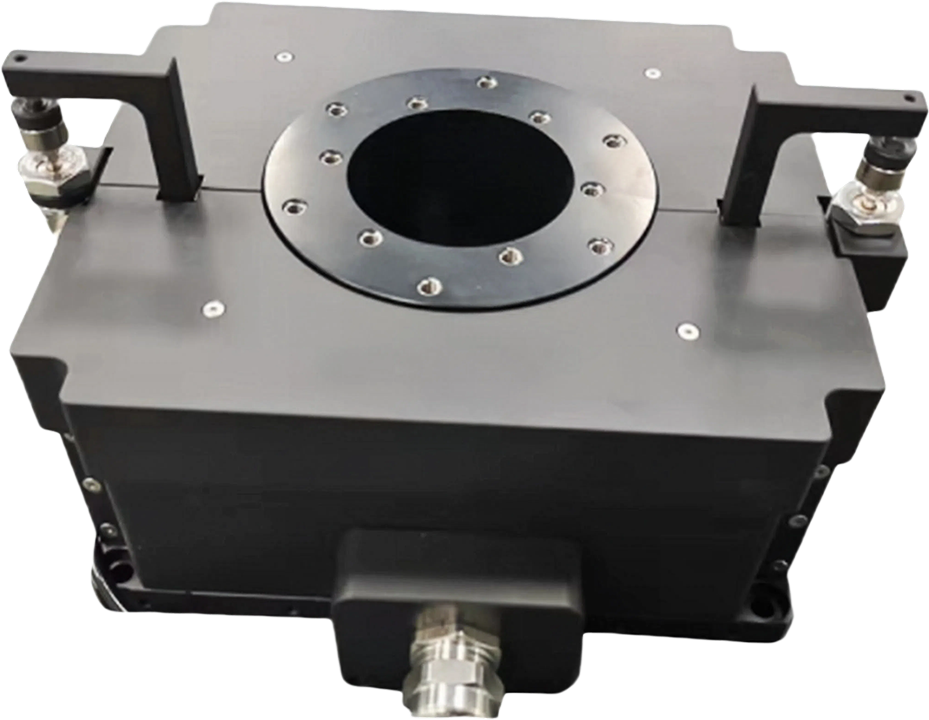
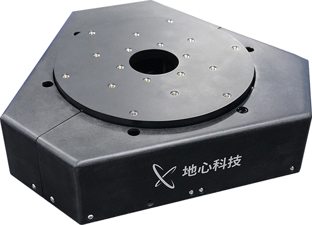
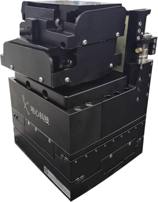
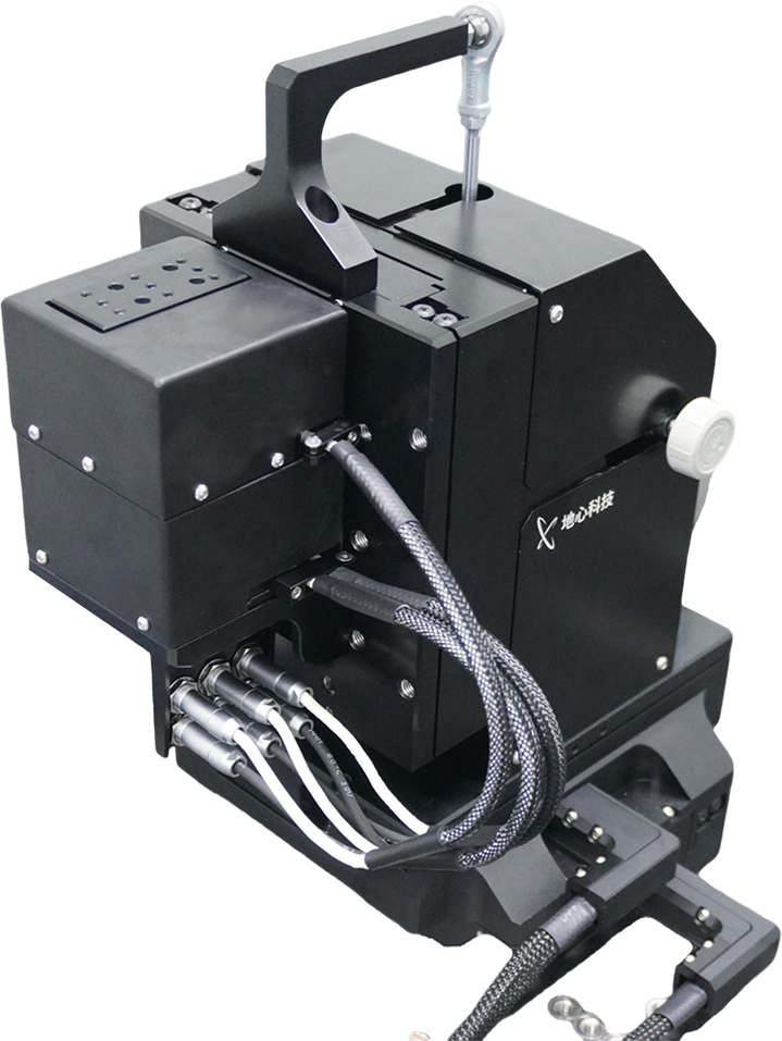
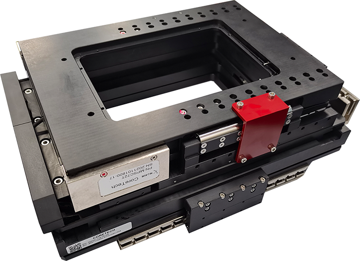
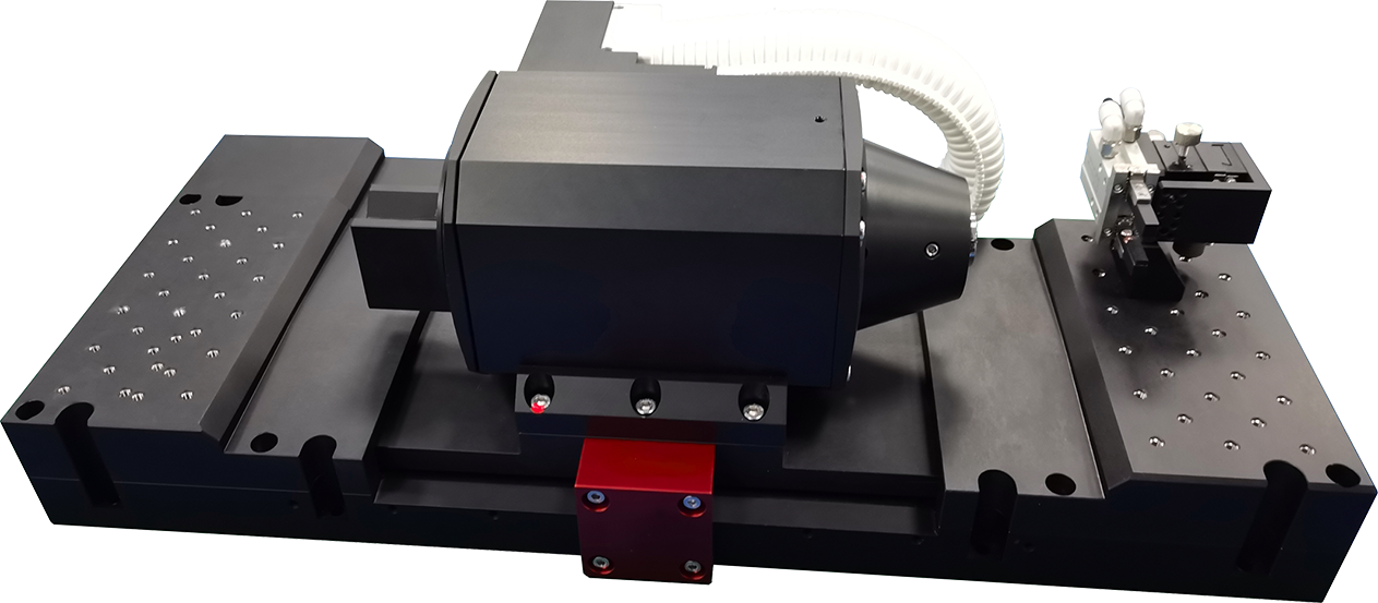
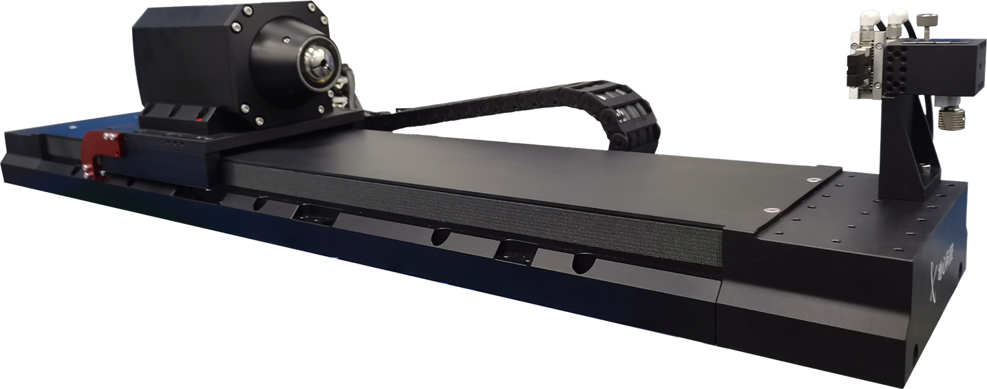
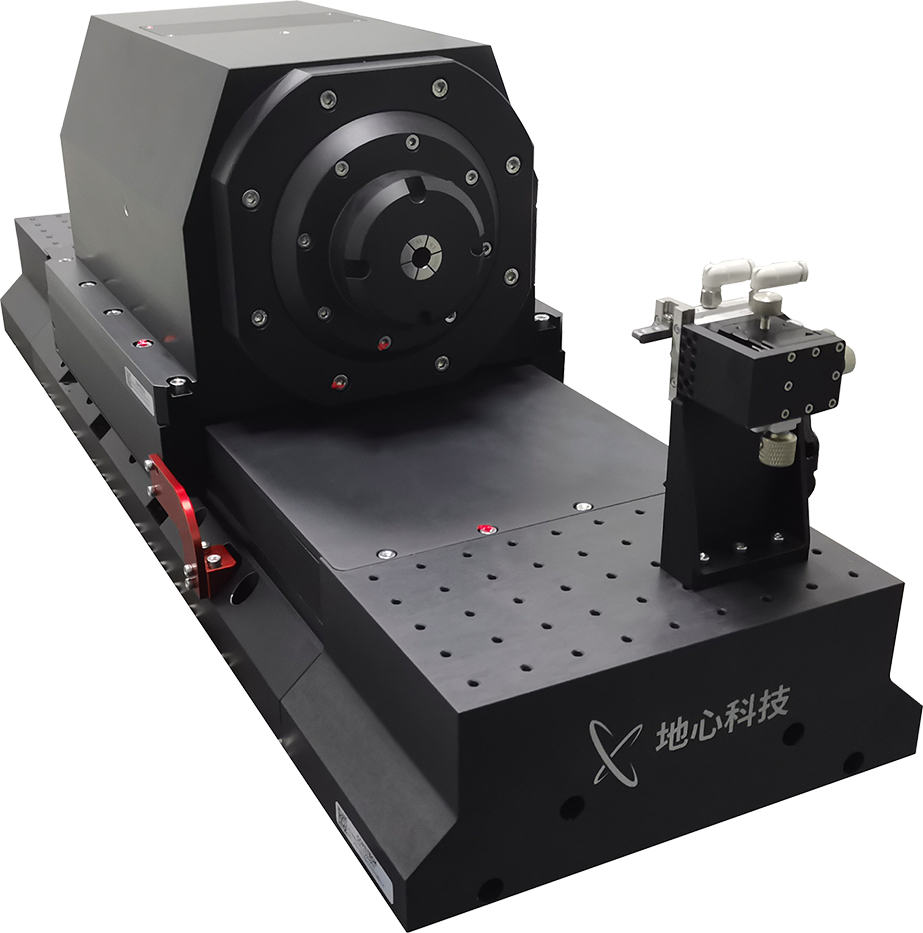
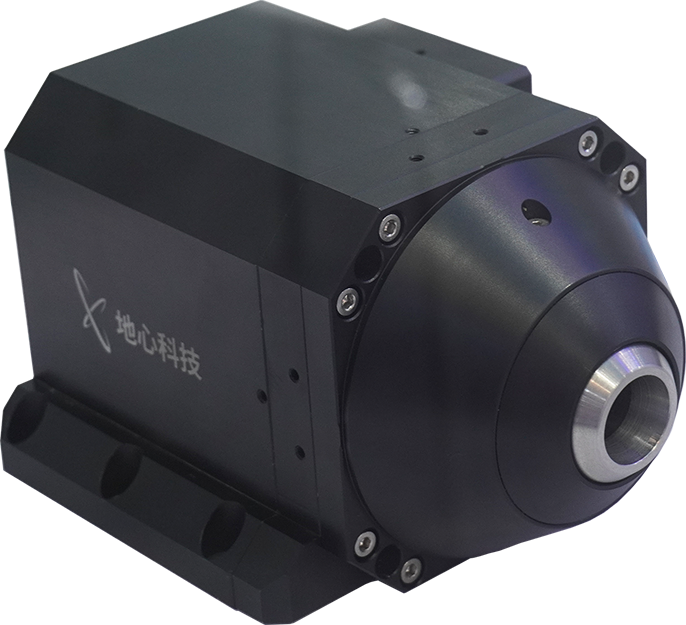
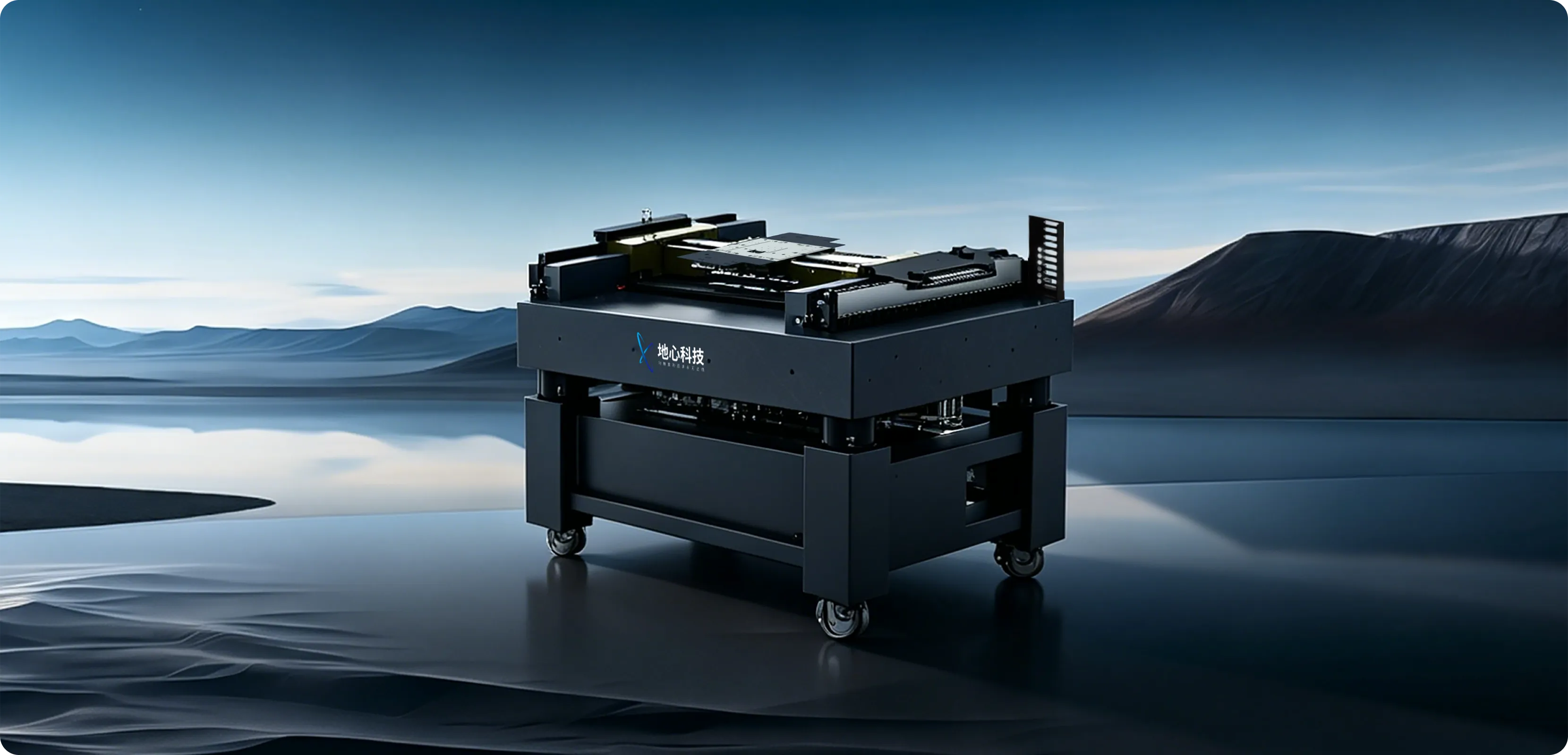
To address wafer surface defect and dimensional inspection needs, CoreTech offers a range of motion stages with diverse performance options for automated inspection equipment integrators. Supported inspection modes include serpentine on‑the‑fly linear scanning, area‑array camera point‑to‑point region inspection, and high‑speed spiral trajectory scanning—enabling accurate and efficient wafer screening.
Recommended Products


Empowerment Case Studies
.webp)
.png)
.webp)
One Article Summary | Multiple Applications of Precision Motion Stages in Wafer Defect Inspection


Breaking the Boundaries of Chip Yield Improvement: Geocentric Technology's Wafer Spiral Inspection Solution Accelerates Quality and Efficiency in the Industry
Wafer Defect Inspection: Solving the "Auto‑Focus Tracking" Challenge to Improve Detection Accuracy and Efficiency


Technical Resources
One‑Stop Product Resource Center


After‑Sales Service
Full‑Cycle Continuous Support


FAQs
Quick Answers to Common Questions

Need engineer assistance for product selection or a quote?
Contact us to create your customized precision motion solution.
Leave a message now


Submit Form